STM32 GPIO Speed and Output Drive
In the GPIO panel of STM32CubeMX, every output pin has a drop-down called Maximum output speed with the options Low, Medium, High, and Very High. Many beginners read this as a performance setting and choose Very High for every pin, expecting the pin to respond faster or the code behind it to run faster. The setting has nothing to do with the CPU. It changes how steeply the output driver moves the voltage from one logic level to the other, and that affects signal quality, electrical noise, and the current spikes on the supply.
In this article, we will see why GPIO speed is an electrical property of the pin.. We will begin with the difference between GPIO speed and CPU speed, and then cover rise time, fall time, and edge rate, followed by the speed options on STM32 devices and the current limits of an output pin. In the later sections, we will deal with EMI and power consumption, choosing a setting for a given signal, and measuring the result on a NUCLEO-F446RE board.
This article is part of the STM32 GPIO tutorial series.
Table of contents
What Is STM32 GPIO Speed?
When a GPIO pin is configured as an output, or as an alternate function such as the clock line of an SPI peripheral, a small driver circuit inside the microcontroller changes the voltage on the pin. As described in the push-pull vs open-drain article, a push-pull driver contains one transistor that connects the pin to the supply and another that connects it to ground. The speed setting adjusts how aggressively this driver switches between the two states.
At the register level, every pin has a two-bit field in the output speed register, which is called GPIOx_OSPEEDR on the STM32F4 series.
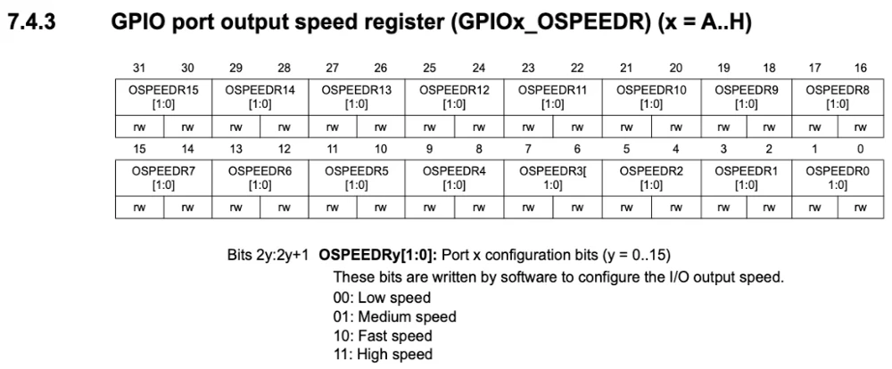
The reference manual calls the four values Low, Medium, Fast, and High, and CubeMX shows them as Low, Medium, High, and Very High.
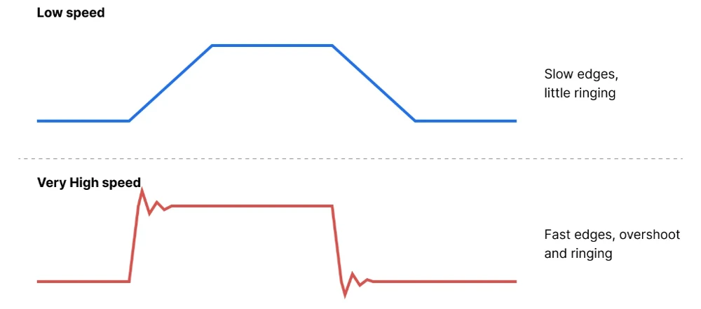
The setting changes the slew rate of the output, which is the rate at which the voltage changes during a transition. A lower setting produces a slower and gentler edge, and a higher setting produces a faster and sharper edge. The logic levels and the data that the pin carries stay the same in both cases, and only the shape of the transition between the two levels is different.
Because the setting belongs to the output driver, it has no effect on a pin that is configured as an input or as an analog pin. This is the reason why CubeMX did not generate a speed field for the PA0 button input in the pull-up and pull-down article, while it did generate one for the output pin on PA5.
GPIO Speed vs CPU Speed
The name of the setting is the main reason it gets confusing. STM32CubeMX labels it Maximum output speed and has options for Low, Medium, High, and Very High. This seems like a choice about how fast the microcontroller runs. The CPU and the GPIO output speed are in fact two separate things, and each one acts at a different point between the software and the pin.
The CPU clock determines how quickly instructions are executed, and therefore how often software can write to the GPIO registers. The GPIO speed setting acts at the opposite end of the path. After a register has been written, the speed setting decides how quickly the output driver moves the voltage at the pin to the new level. The diagram below shows the two parts of the path.
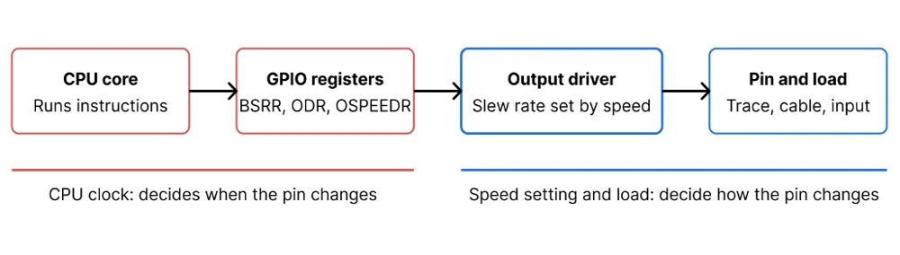
Let’s understand this using an example. A CPU running at 180 MHz can write to a port register in a few nanoseconds, but a pin that is set to Low speed and connected to a capacitive load can need considerably longer to complete the transition. The software has finished its work long before the voltage at the pin reaches the new level, and this delay is a property of the driver and the load rather than of the processor.
The reverse is also true. Setting a pin to Very High does not make the CPU run faster, and it does not increase the rate at which software can toggle the pin. The toggle rate is determined by the code and by the system clock, which is covered in the STM32 Clock System Explained article. The speed setting only determines how fast a toggling signal can be before its waveform starts to degrade.
STM32 GPIO Rise Time and Fall Time
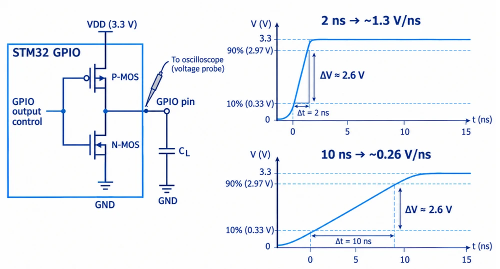
An ideal digital signal would jump from LOW to HIGH in no time at all. A real pin cannot do this, because the output driver has a finite output resistance and the pin is connected to some capacitance. This capacitance includes the pin itself, the PCB trace, any cable, and the input of the device at the other end. The driver has to charge this capacitance to raise the voltage and discharge it to lower the voltage. Both these actions take a measurable amount of time.
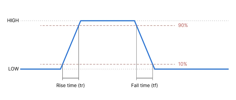
Rise Time and Fall Time
Rise time is basically the time that the signal needs to move from 10 percent to 90 percent of its full swing on a rising edge. Similarly, Fall time is the same measurement, but on a falling edge. Some datasheets use the 20 percent and 80 percent points instead, so you must check the definition before comparing the two numbers. The two values are often slightly different, because the transistor that pulls the pin up and the transistor that pulls it down do not have identical characteristics.
Edge Rate
Edge rate describes how quickly the voltage changes during a transition, and it is the same behavior that rise time measures, expressed as a slope. It is calculated by dividing the change in voltage by the time the change takes, and it is usually given in volts per nanosecond. For example, a 3.3 V output that covers 80 percent of its swing (2.6 V) in 2 ns, has an edge rate around 1.3 V/ns. Therefore a shorter rise time gives a higher edge rate, and the two terms are often used interchangeably when the speed setting is discussed.
The edge rate matters because a fast edge behaves like a high-frequency signal, even when the pin toggles slowly. A pin that switches only once per microsecond still makes a very quick jump in voltage during each edge. The electronics around it react to that quick jump, and not to how often it happens. The steeper the edge is, the higher the frequency it can affect.
A common rule of thumb estimates this frequency as 0.35 divided by the rise time. For a rise time of 2 ns, the result is about 175 MHz, even though the pin itself toggles at only 1 MHz. A trace on the board can radiate a frequency like this much more easily than 1 MHz. This is the main reason why a fast speed setting increases EMI. The topic is covered in more detail later in this article.
What Sets the Edge Time
A simple way to estimate the edge time is to treat the output driver as a resistor that charges a capacitor. The rise time is then about 2.2 times the resistance, multiplied by the capacitance. For a driver resistance of 50 Ω and a load of 20 pF, this gives about 2.2 ns.
A real output stage is more complicated than a single resistor, because the speed setting also changes how the transistors turn on, but the estimate still shows the two things that matter. One is how strong the driver is, and the other is how much capacitance it has to charge. A higher speed setting makes the driver switch faster, and a larger load makes every edge slower at any setting.
STM32 GPIO Speed Settings
STM32CubeMX lists the speed options in the GPIO configuration panel under System Core. The table below shows the four options that are available on many families, including the STM32F4 series used in this tutorial series, together with the matching HAL constants.
| CubeMX option | HAL constant | Edge behavior | Typical use |
|---|---|---|---|
| Low | GPIO_SPEED_FREQ_LOW | Slowest edges, lowest noise | LEDs, enable lines, slow control signals |
| Medium | GPIO_SPEED_FREQ_MEDIUM | Moderate edges | UART, I²C, low-speed SPI |
| High | GPIO_SPEED_FREQ_HIGH | Fast edges | SPI at moderate clock rates, timer outputs |
| Very High | GPIO_SPEED_FREQ_VERY_HIGH | Fastest edges, most noise | Fast SPI, SDIO, FMC, and other high-frequency buses |
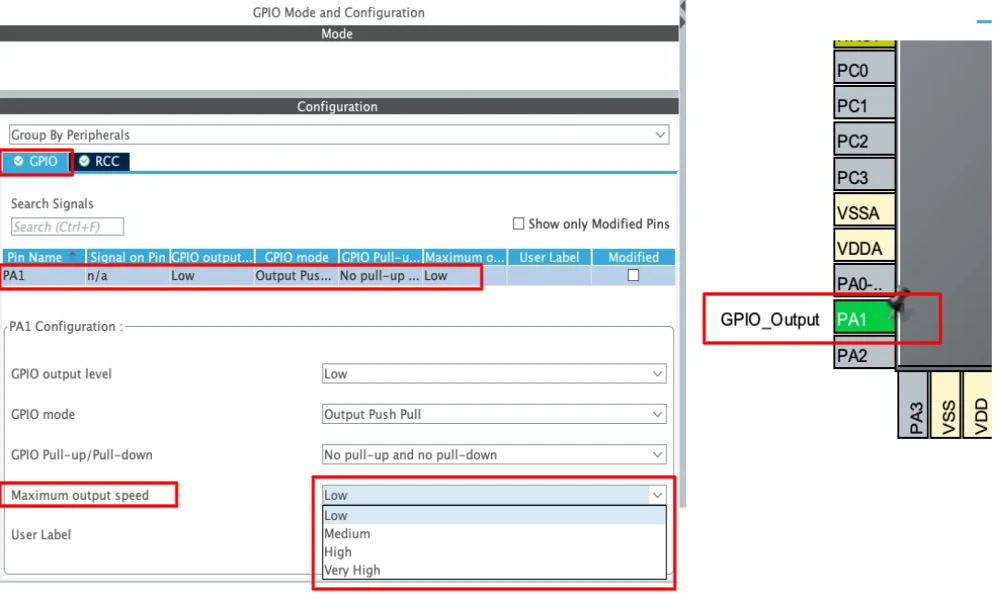
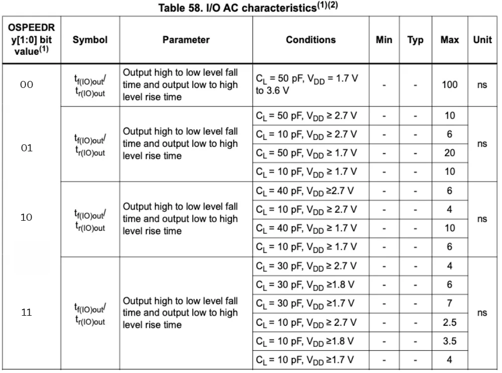
The available choices depend on the STM32 family. Older families such as the STM32F1 offer three options, which are named after the maximum frequency of 2 MHz (Low), 10 MHz (Medium), and 50 MHz (High). Newer families such as the STM32F4, STM32L4, and STM32G4 use the four-level scheme shown above. The actual maximum frequency that corresponds to each level is different from one device to another, and it also depends on the supply voltage and on the load capacitance. The datasheet of the specific chip lists these values in the I/O AC characteristics table, and each value is given for a stated load.
Some families add a further detail for the highest speeds. A few devices include an I/O compensation cell that can be enabled to keep the edge behavior consistent across temperature and voltage, and the reference manual of the device describes when it is needed. If the datasheet of your chip mentions this cell, it is worth reading that section before running a bus at its maximum frequency.
CubeMX also chooses a default speed for pins that belong to a peripheral, and the default is often a middle or high value. This default is a reasonable starting point, but it is not always the best one for a specific board, and it can be changed in the same panel.
STM32 GPIO Output Drive Capability
The speed setting changes how fast the voltage switches, but it does not change how much current the pin can supply. Output drive capability is a separate property, and it is limited by the size of the transistors in the output stage and by the rules in the datasheet.
Source and Sink
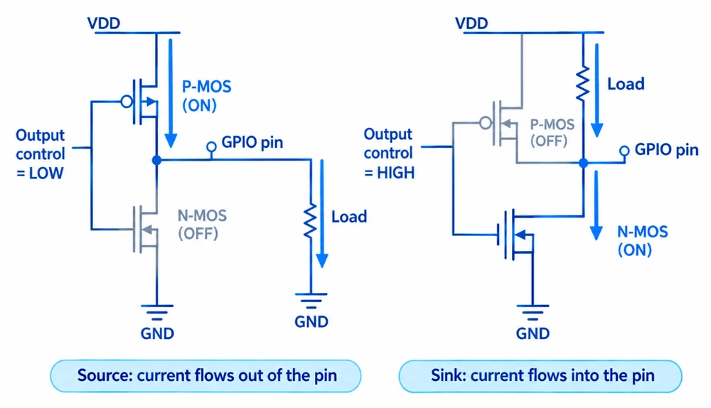
A push-pull output can deliver current in two directions. When the pin is HIGH, the upper transistor is on, and the pin supplies current to the load, which is called sourcing. When the pin is LOW, the lower transistor is on, and the pin takes in current from the load, which is called sinking. The two cases are shown in the diagram below.
Electrical Limits
The transistors in the output stage have a small but real resistance, so the output voltage changes as the load current changes. When a pin sources current, the HIGH level falls below the supply voltage, and when it sinks current, the LOW level rises above 0 V. The datasheet describes this with the VOH and VOL specifications, which are guaranteed only up to a stated current, for example 8 mA. Many devices also list a higher current for which the levels are relaxed. Beyond these values, the output voltage may no longer be recognized as a valid logic level by the device that it drives.
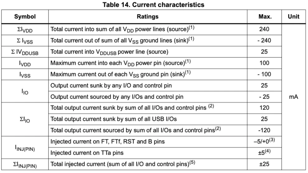
The datasheet also lists absolute maximum ratings. These include a maximum current for a single pin, and on the STM32F4 series this is in the range of 25 mA, together with a limit for the total current of all pins on the device. An absolute maximum rating is a limit that must not be exceeded, and it is not a value that is safe for normal operation. In practice, a pin should be used at a current well below the guaranteed VOH and VOL current, and the total current of all pins should be kept below the limit for the package.
Driving Loads
A GPIO pin is a signal output and not a power output, which means that it should drive loads that need only a few milliamps. A small LED with a series resistor is a good example, because a 330 Ω resistor and an LED on a 3.3 V supply draw about 4 mA. Loads such as relays, motors, solenoids, buzzers, and long strings of LEDs draw much more current than a pin can deliver. These loads should be driven through a transistor or a MOSFET, with the GPIO pin only switching the control input. An inductive load such as a relay coil or a motor also needs a flyback diode, because it produces a voltage spike when the current is switched off.
The speed setting does not help in this situation. Setting a pin to Very High makes the edges faster, but it does not raise the current limit of the pin, and a pin that is overloaded at Low speed is still overloaded at Very High speed.
GPIO Speed, Power and EMI
The speed setting is a trade-off between signal timing on one side and noise and power on the other side. The chain below summarizes how these effects are connected.

EMI and Ringing
As explained earlier, a fast edge contains high-frequency energy, and a PCB trace or a cable can radiate this energy like a small antenna. A faster edge therefore increases the electromagnetic emissions of the board, even when the signal itself toggles slowly. Fast edges can also excite the inductance of a trace and the capacitance of the load, which produces ringing. Ringing appears as overshoot above the HIGH level and undershoot below the LOW level, and in a bad case it can cross the input threshold of the receiver more than once and cause false edges. Overshoot beyond the supply rails can also stress the protection diodes of the receiving pin.
Power and Supply Noise
The average power that a pin uses to drive a load depends mainly on the load capacitance and on how often the pin switches. It can be estimated with the formula P = C × VDD² × f, where C is the load capacitance, VDD is the supply voltage, and f is the switching frequency. For a 20 pF load on a 3.3 V supply that switches at 10 MHz, the result is about 2.2 mW, and this value is almost the same for every speed setting.
The speed setting has a much larger effect on the peak current than on the average power. A faster edge moves the same charge in less time, so the current reaches a higher peak. During the transition, both output transistors can also conduct for a very short moment, which adds to the spike. These spikes travel through the supply and ground connections and can disturb other parts of the chip and the board, especially when many pins switch together, as on a parallel bus. Decoupling capacitors placed close to the supply pins reduce the effect, and a lower speed setting reduces the spike itself.
How to Choose the Right GPIO Speed
The general rule is to select the lowest speed setting that meets the timing of the signal with some margin. A slower edge produces less EMI, less ringing, and smaller current spikes, and it costs nothing as long as the signal still settles well before the receiver samples it. Choosing a setting that is too low causes the opposite problem. The edges become so slow that the signal has not finished changing when the next edge begins. The receiver may then read the wrong level, or it may sample the signal too early or too late for its setup and hold times.
The table below gives a starting point for common signals. The values are not strict limits, since the load, the supply voltage, and the family all influence the result. Always consult the datasheet for the final decision.
| Signal | Typical frequency | Suggested starting point |
|---|---|---|
| LED or relay driver input | Static or a few Hz | Low |
| Enable, reset, and chip-select lines | Static or slow | Low |
| UART | Up to a few Mbit/s | Low or Medium |
| I²C | 100 kHz to 1 MHz | Low or Medium |
| SPI | A few MHz to 20 MHz | Medium or High |
| SPI, SDIO, and FMC at the top of their range | 40 MHz and above | High or Very High |
Long wires and large loads make the choice harder, because they push the setting in two directions. A long cable adds capacitance, which slows down the edges, so a higher setting may be needed to keep the signal within its timing limit. A long trace without termination is also more likely to ring, and this is a reason to keep the setting as low as the timing allows.
For a fast bus, the better approach is to keep the traces short and to place a small series resistor near the pin, which is called a series termination resistor. The resistor dampens the ringing and gives a cleaner edge. The speed setting should then be used only for the final adjustment.
STM32 GPIO Speed Example
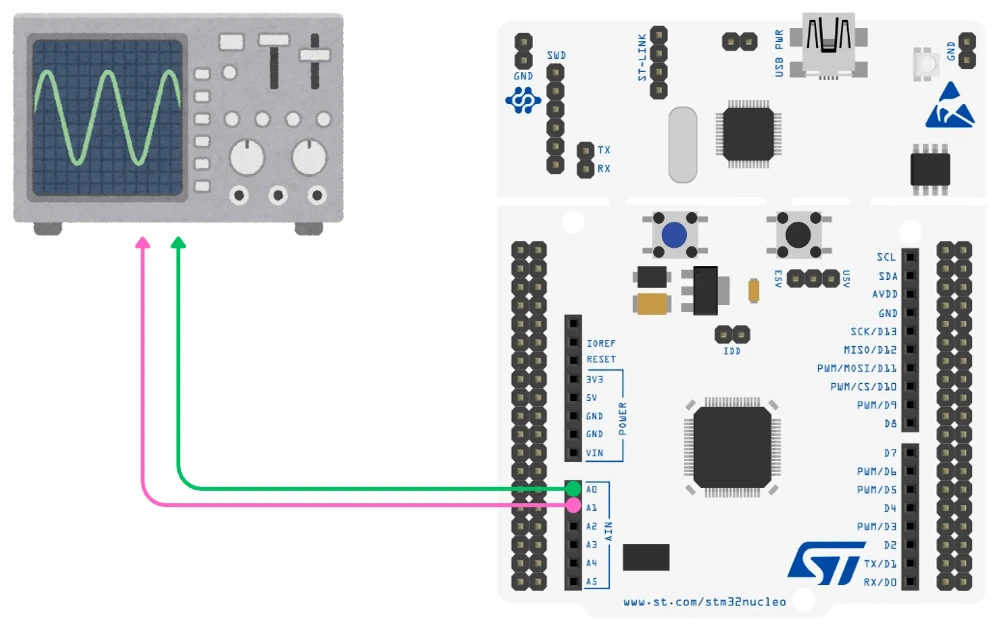
This example toggles two output pins at the same time with identical code. PA0 is set to Low speed and PA1 is set to Very High speed, so the only difference between the two signals is the output speed setting. The example uses a NUCLEO-F446RE board, and the two signals can be observed on an oscilloscope with PA0 and PA1 on two channels and a shared ground.
Step 1: Configure the Pins
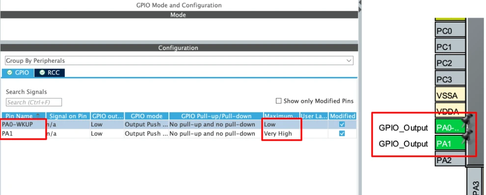
In the Pinout & Configuration tab, set PA0 and PA1 to GPIO_Output. Then open System Core → GPIO and use the settings in the table.
| Setting | PA0 | PA1 |
|---|---|---|
| GPIO mode | Output Push Pull | Output Push Pull |
| GPIO Pull-up/Pull-down | No pull-up and no pull-down | No pull-up and no pull-down |
| GPIO output level | Low | Low |
| Maximum output speed | Low | Very High |
Step 2: The Generated Code
CubeMX writes the pin setup into MX_GPIO_Init() in main.c. The only difference between the two pins is the Speed field.
|
1 2 3 4 5 6 7 8 9 10 11 12 13 |
/*Configure GPIO pin : PA0 */ GPIO_InitStruct.Pin = GPIO_PIN_0; GPIO_InitStruct.Mode = GPIO_MODE_OUTPUT_PP; GPIO_InitStruct.Pull = GPIO_NOPULL; GPIO_InitStruct.Speed = GPIO_SPEED_FREQ_LOW; HAL_GPIO_Init(GPIOA, &GPIO_InitStruct); /*Configure GPIO pin : PA1 */ GPIO_InitStruct.Pin = GPIO_PIN_1; GPIO_InitStruct.Mode = GPIO_MODE_OUTPUT_PP; GPIO_InitStruct.Pull = GPIO_NOPULL; GPIO_InitStruct.Speed = GPIO_SPEED_FREQ_VERY_HIGH; HAL_GPIO_Init(GPIOA, &GPIO_InitStruct); |
Step 3: Add the Application Code
The loop below writes to the BSRR register directly instead of calling HAL functions. A HAL call adds overhead, which would slow the toggle rate, and two separate calls would also change the pins at slightly different times. A single BSRR write changes both pins in the same instruction, so PA0 and PA1 switch together and the toggle rate stays as high as possible. The lower 16 bits of BSRR set pins, and the upper 16 bits reset them. Add the code between the USER CODE BEGIN 3 markers.
|
1 2 3 4 5 6 7 8 9 |
while (1) { /* USER CODE END WHILE */ /* USER CODE BEGIN 3 */ GPIOA->BSRR = GPIO_PIN_0 | GPIO_PIN_1; // both pins HIGH GPIOA->BSRR = (uint32_t)(GPIO_PIN_0 | GPIO_PIN_1) << 16U; // both pins LOW } /* USER CODE END 3 */ |
Keep all custom code between the USER CODE markers, or CubeMX will delete it the next time you regenerate the project.
Step 4: Build, Flash, and Observe
Click Build and then Run. On the scope, both channels show a square wave with the same frequency, because the same instruction drives both pins. However, the two edges are different. The PA0 trace, which uses Low speed, has visibly slower rising and falling edges. On the other hand, the PA1 trace, which uses Very High speed, has steeper edges and may show some overshoot. The exact toggle frequency depends on the system clock and on the compiler settings, so it should be measured and not assumed.
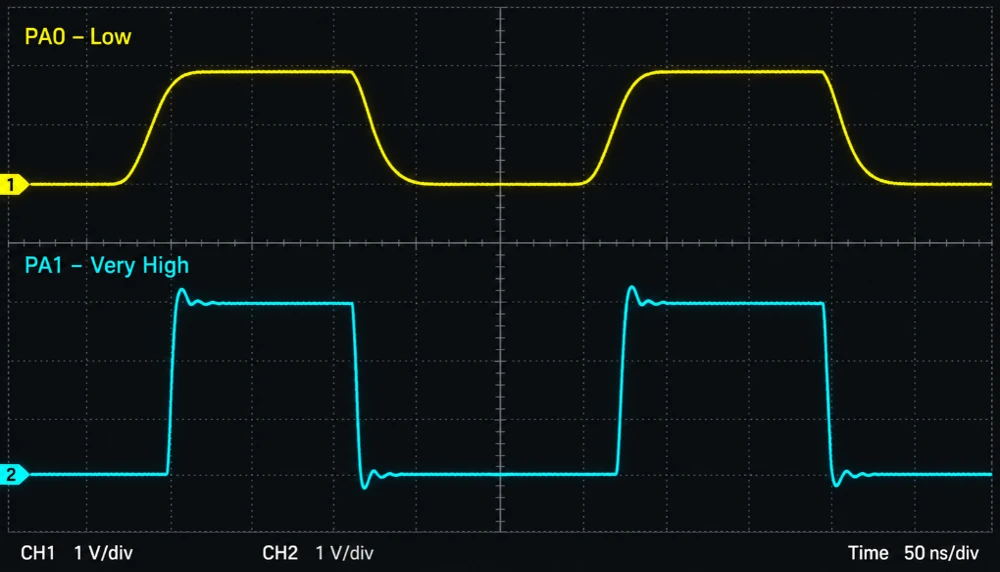
A longer jumper wire on the pins makes the difference easier to see, because the added capacitance slows down the edges of both pins. Without a scope, a logic analyzer can still confirm that both pins toggle at the same frequency, which supports the main point of this article that the speed setting does not change the rate of the code.
Conclusion
The GPIO speed setting controls the slew rate of the output driver, which means that it decides how fast the voltage at a pin moves between LOW and HIGH. It does not change how fast the CPU runs, it does not set the toggle frequency, and it does not increase the current that the pin can deliver. The rise time and fall time that result from the setting depend on both the driver and the load, and they determine how much high-frequency content the signal contains.
A faster setting is necessary for high-frequency buses, where the edges must be short enough for the receiver to sample the data correctly. For most other signals, it only adds EMI, ringing, and supply noise. A good habit is to choose the lowest speed that meets the timing of each signal with some margin, and to confirm the choice with the datasheet and, when possible, with a measurement. The output current is a separate topic, and the pin should drive only small loads, with a transistor or a MOSFET used for anything that needs more current than the datasheet allows.
Download the Project Here
Download the CubeMX project files and HAL source code — all tested on real hardware.
If you find this useful, you can support us with a Donation as well.