STM32 Clock System Explained
If you have gone through the previous guides in this series, you have already generated a project, flashed it onto a board, and watched an LED blink with a delay. That LED blinked once every second because of a line that said HAL_Delay(1000). But have you ever wondered how the chip actually knows how long a millisecond is?
The answer is the clock system. Every single thing your STM32 does, from toggling a pin to sending a UART byte to sampling an ADC channel, happens in time with a clock signal ticking inside the chip. If you do not understand the clock system, a lot of STM32 behaviour just won’t make sense. A UART that prints garbage. A timer that runs twice as fast as you expected. A delay that is way off. Most of the time, the real problem is a clock setting, not your logic.
This guide is going to walk you through the STM32 clock system from the ground up. We will look at where the clock actually comes from, how it gets multiplied and divided on its way to your peripherals, and how to read and set all of this inside STM32CubeMX. By the end, you should be able to look at a clock tree diagram and actually know what you are looking at, instead of just clicking buttons and hoping.
Table of contents
- STM32 Clock System Explained
- Why Does an STM32 Need a Clock?
- STM32 Clock Sources
- HSI, HSE, LSI and LSE
- PLL and the System Clock
- STM32 Clock Tree Explained
- AHB and APB Bus Clocks
- Peripheral Clock Enable
- Timer Clock vs APB Clock
- How to Calculate Peripheral Frequencies
- Clock Configuration in STM32CubeMX
- Working Example: Watching the Clock Affect Timing
- Wrapping Up
Why Does an STM32 Need a Clock?
A microcontroller needs a steady, repeating signal to keep everything happening at the right moment, in the right order. Every instruction the CPU runs, every bit that goes out on UART, every sample the ADC takes, needs to happen at a steady, known rate. Without a clock, none of that timing exists.
The clock is what turns a chip full of transistors into something that behaves predictably. It is also what lets different parts of the chip talk to each other correctly. If your UART peripheral expects a bit every so many microseconds, and its clock is wrong, the receiving device on the other end will read garbage, even though your code looks completely fine.
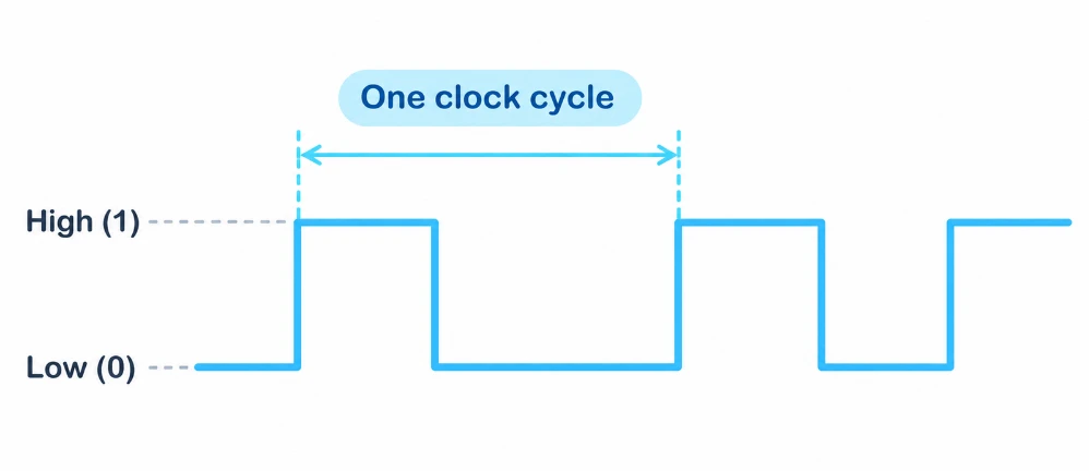
This is really the whole reason clock configuration matters so much on STM32. It is not just background setup you do once and forget. It directly decides how fast your code runs, how accurate your delays are, and whether your peripherals talk to the outside world correctly.
STM32 Clock Sources
An STM32 chip does not generate its own timing out of nothing. It needs a clock source, something that produces a steady, repeating signal the rest of the chip can work with. STM32 chips give you more than one option here, and that is actually a good thing, because different situations call for different trade-offs between accuracy, cost, and power.
Broadly, you have two kinds of clock sources on almost every STM32:
- Internal oscillators, built right into the chip. No external parts needed.
- External oscillators, using a crystal or resonator you add to your board.
Internal sources are easy. You do not need to add anything to your circuit, and they start up fast. The trade-off is accuracy. They drift a bit with temperature and are not as precise over time.
External sources need an extra crystal on your PCB, but they are far more accurate and stable, which matters a lot once you start doing things like UART communication at higher baud rates or USB, where timing accuracy is non-negotiable.
| Internal Oscillator (HSI/LSI) | External Oscillator (HSE/LSE) | |
|---|---|---|
| Extra hardware needed | None | Crystal or resonator required |
| Startup time | Fast | Slower (crystal needs to stabilize) |
| Accuracy | Lower, drifts with temperature | High, stable over time |
| Cost | Free (built into chip) | Adds a small cost to the BOM |
| Best for | Quick prototyping, non-critical timing | UART, USB, RTC, anything timing-sensitive |
HSI, HSE, LSI and LSE
STM32 chips name their clock sources with short acronyms, and once you know what each one stands for, they stop being confusing.
- HSI (High-Speed Internal): an internal oscillator, usually running at 8 MHz, 16 MHz or even at 64MHz depending on the chip family. No external hardware needed. It is what your chip uses right after reset, before you configure anything else.
- HSE (High-Speed External): a clock source that comes from outside the chip, usually a crystal in the 4 MHz to 26 MHz range, sometimes even higher. It is more accurate than HSI, and it is the usual choice when you care about precise timing.
- LSI (Low-Speed Internal): a small internal oscillator, usually around 32 kHz. It is mainly used for the independent watchdog timer and for RTC backup when no external crystal is fitted.
- LSE (Low-Speed External): an external 32.768 kHz crystal, the same kind you would find in a wristwatch. This is the standard choice for driving the real-time clock (RTC) accurately.
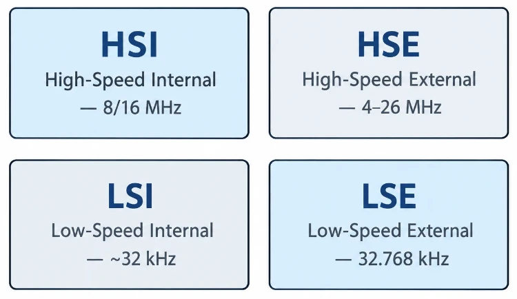
HSI and HSE are not for the same job as LSI and LSE. The “high-speed” ones drive your CPU and most peripherals. The “low-speed” ones are for things that need to keep ticking accurately over long periods, like a watchdog or a real-time clock, without needing to run fast.
By default, most STM32 projects use HSI right after startup. Then they switch to HSE (if a crystal is fitted) or stick with HSI, and feed that into the PLL to get a higher and more useful clock speed.
PLL and the System Clock
HSI and HSE on their own are usually not fast enough. For example, an STM32F4 chip can run its CPU well above 100 MHz, but HSE crystals are commonly only 8 MHz or 25 MHz. You need something in between that takes a slower input clock and turns it into a much faster one. That thing is the PLL (Phase-Locked Loop).
You do not need to understand the electronics behind a PLL to use one. Just think of it as a frequency multiplier with some knobs on it. You feed it an input clock, usually HSI or HSE, and it multiplies that up to a higher frequency using a set of configurable ratios. On most STM32 families, those ratios have names like PLLM, PLLN, and PLLP (or similar, depending on the family).
Here is how it works:
- The input clock first gets divided down by PLLM, to land in a range the PLL likes to work with, usually around 1-2 MHz.
- That result gets multiplied up by PLLN, to a much higher internal frequency.
- That high internal frequency then gets divided down again by PLLP, to produce the final system clock.
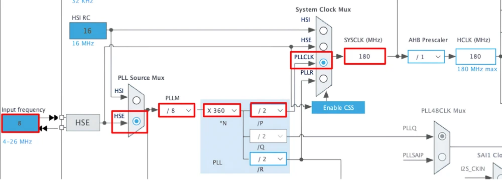
The output of this whole chain becomes your SYSCLK, the system clock. This is the clock that drives your CPU core and feeds into everything else on the chip, through the clock tree we are about to look at.
You do not need to calculate these values by hand. STM32CubeMX does the math for you and even warns you if you pick numbers that push a peripheral above its maximum rated frequency. But it helps a lot to understand what those PLLM, PLLN, and PLLP fields inside CubeMX are actually doing, instead of just typing in whatever value gets you the frequency you want.
STM32 Clock Tree Explained
Once you have SYSCLK, it doesn’t go straight to every peripheral at the same speed. It splits into branches, and each branch has its own divider, called a prescaler, that slows the clock down before it reaches a particular part of the chip. This branching structure, from SYSCLK down to the individual peripherals, is called the clock tree.
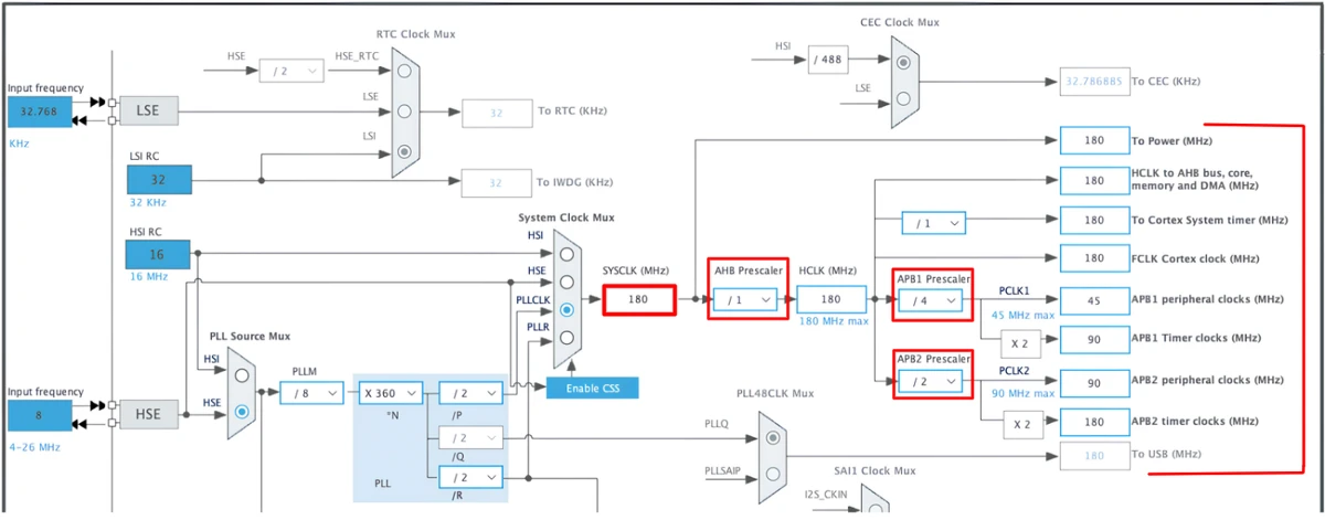
The general path is as follows:
- SYSCLK feeds the AHB bus, through the AHB prescaler.
- The AHB bus clock feeds the APB1 and APB2 buses, each through their own prescaler.
- Each APB bus then feeds a group of peripherals connected to it.
This branching is exactly why two peripherals on the same chip can run at two completely different speeds, even though they both ultimately trace back to the same SYSCLK. It all depends on which bus they sit on, and what prescaler value is set for that bus.
AHB and APB Bus Clocks
The AHB (Advanced High-performance Bus) is the main internal highway of the chip. It carries the clock that drives the CPU core itself, along with memory and a handful of high-speed peripherals like GPIO ports and DMA.
Below AHB, you typically find two APB (Advanced Peripheral Bus) branches, called APB1 and APB2. These carry the clock further out to most of your peripherals, things like USART, SPI, I2C, and timers.
Why two separate APB buses instead of one? Mainly for flexibility and to keep the electrical loading on each bus manageable. APB2 is usually allowed to run faster than APB1 on many STM32 families, and STMicroelectronics splits peripherals between the two based on typical speed needs. High-speed peripherals like ADC and certain timers tend to sit on APB2. Slower or less timing-critical ones tend to sit on APB1.
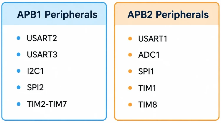
Each of these buses has its own prescaler, which divides down the AHB clock before it reaches that bus. So if AHB is running at 180 MHz and the APB1 prescaler is set to divide by 4, every peripheral sitting on APB1 sees a base clock of 45 MHz, not 180 MHz. This single fact is usually the real reason behind a wrong baud rate or a timer running at half the speed than expected.
Peripheral Clock Enable
Here is something that catches a lot of people the first time they write STM32 code without CubeMX doing it for them: peripherals on an STM32 chip are off by default, even after you have correctly configured the clock tree.
Having a clock reach a peripheral is not enough. That peripheral also needs its clock explicitly turned on, through a clock enable bit, before it will do anything at all. If you forget this step, the peripheral simply does not respond, and it will look exactly like broken hardware, even though nothing is actually wrong.
In HAL code, this shows up as function calls like:
|
1 2 3 |
__HAL_RCC_GPIOA_CLK_ENABLE(); __HAL_RCC_USART2_CLK_ENABLE(); __HAL_RCC_TIM3_CLK_ENABLE(); |
When you enable a peripheral inside STM32CubeMX, whether that is a GPIO pin, a USART, or a timer, CubeMX automatically adds the correct clock enable call for you inside the generated MX_..._Init() function. You do not have to remember to add these lines yourself in a CubeMX-based project. But it is worth knowing they exist, because if you ever add register-level code by hand, missing this line is one of the first things to check when a peripheral seems completely unresponsive.
Timer Clock vs APB Clock
This confuses almost everyone the first time they run into it, and the STM32 reference manual explains it in a way that is technically correct but not exactly beginner-friendly.
Here is the short version. If an APB bus prescaler is set to divide by 1, the timers on that bus run at the same frequency as the APB bus clock. But if the APB prescaler is set to anything other than 1 (dividing by 2, 4, or more), the timers on that bus actually get their clock multiplied by 2 relative to that APB clock, not the same speed as the bus.
So the rule is:
- APB prescaler = 1 → Timer clock = APB clock
- APB prescaler > 1 → Timer clock = APB clock × 2
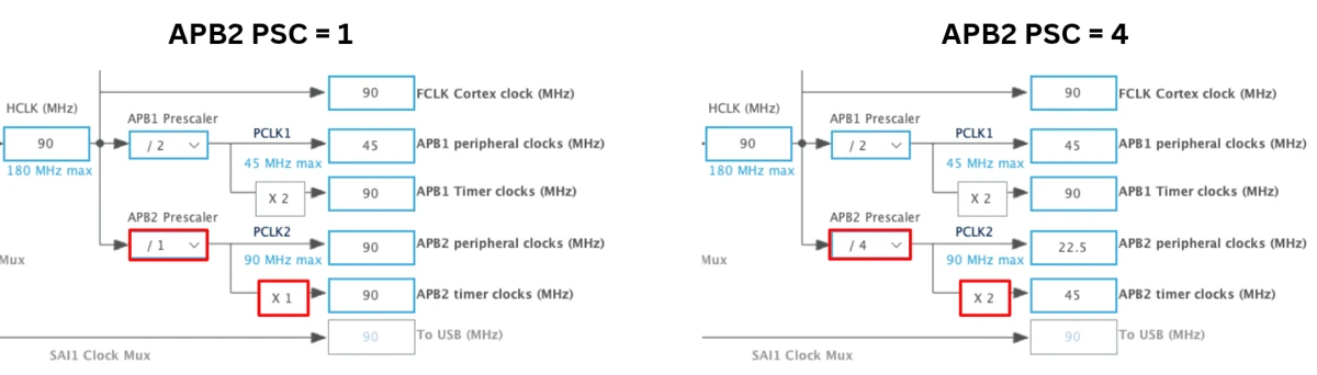
This rule exists so that timers stay usable and predictable even when a bus is divided down for other peripherals. It’s useful once you know about it. But forget it exists, and you’ll end up with a timer running at double the speed you calculated by hand. STM32CubeMX handles this automatically in the clock tree diagram, showing you the real timer clock value, not just the raw APB value, which is one more good reason to lean on CubeMX rather than doing all this math by hand every time.
How to Calculate Peripheral Frequencies
Once you understand the path a clock takes, from HSI or HSE, through the PLL, down through AHB, and out to an APB bus, working out the actual frequency reaching a peripheral is just multiplication and division, one step at a time.
Let’s walk through a real example, using values common on an STM32F4 board running at 180 MHz:
- HSE crystal: 8 MHz
- PLLM divides it down: 8 MHz ÷ 8 = 1 MHz
- PLLN multiplies it up: 1 MHz × 360 = 360 MHz
- PLLP divides it down again: 360 MHz ÷ 2 = 180 MHz → this is SYSCLK
- AHB prescaler = 1 → AHB clock = 180 MHz
- APB1 prescaler = 4 → APB1 clock = 45 MHz
- APB1 timer clock (since prescaler > 1) = 45 MHz × 2 = 90 MHz
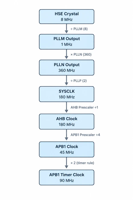
Notice something here. Even though APB1 itself is running at 45 MHz, a timer sitting on APB1 still sees 90 MHz, thanks to that ×2 rule from the last section. This is exactly the kind of calculation that feels confusing written out in a paragraph, but becomes obvious once you have walked through it step by step a couple of times.
Clock Configuration in STM32CubeMX
Everything covered so far can be configured visually inside STM32CubeMX, on the Clock Configuration tab. This is genuinely one of the best parts of CubeMX, because it turns an abstract clock tree into something you can click and drag.
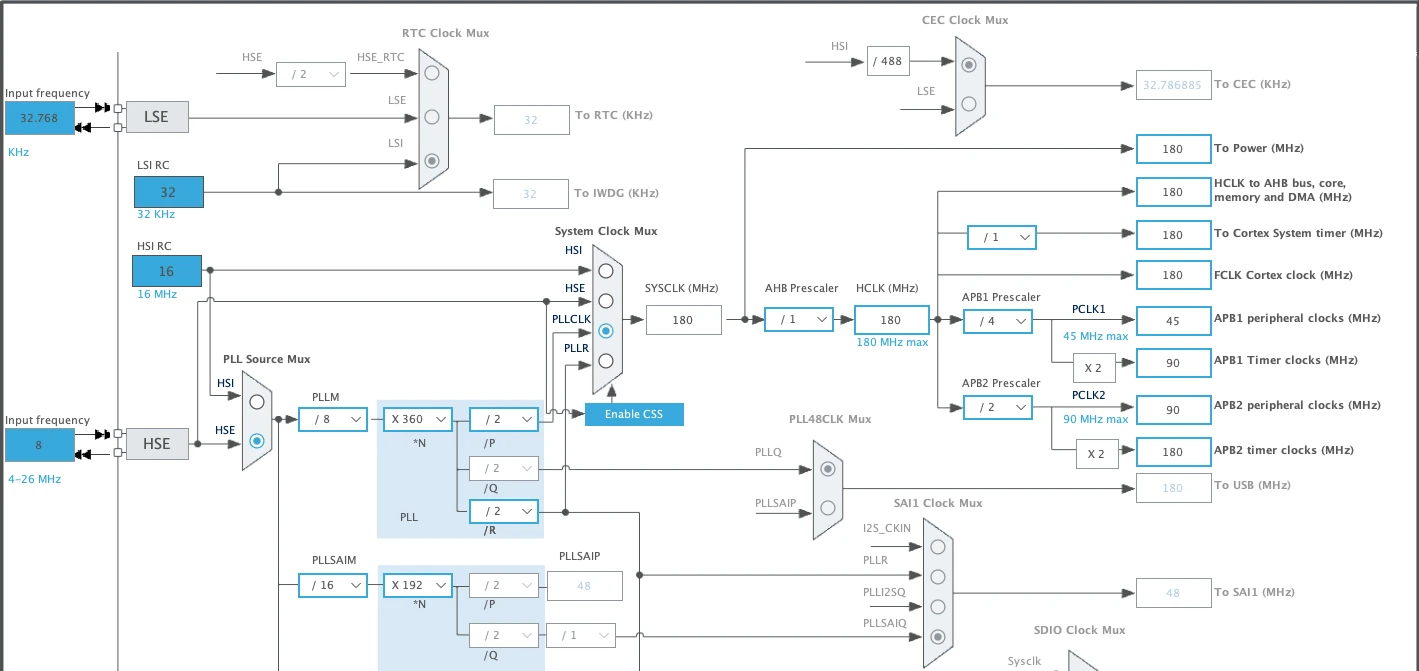
Here is the general flow for setting it up:
- On the Pinout & Configuration tab, enable your clock source (HSE if you have a crystal on your board) under the RCC settings.
- Switch to the Clock Configuration tab. You will see the full clock tree diagram, starting from HSI/HSE on the left.
- Click on the PLL source box and select HSE or HSI as the input.
- Type your target system clock frequency into the SYSCLK box, at the far right. CubeMX will automatically calculate PLLM, PLLN, and PLLP for you, and fill them in.
- Adjust the AHB, APB1, and APB2 prescalers if needed. CubeMX shows the resulting frequency next to each one as you change it.
- If any value goes above what your specific chip supports, CubeMX highlights that field in red. This is one of the most useful safety nets in the whole tool.
Once you are happy with the numbers, generate the code as usual. CubeMX writes all of this into the SystemClock_Config() function inside main.c, which is the function that runs first, right at the top of main(), before anything else.
Working Example: Watching the Clock Affect Timing
Let’s make all of this concrete with a small, working example. We will take the same LED-blinking project from the earlier guides, and change nothing except the clock configuration, just to see the timing actually shift in front of you.
- Open your existing CubeMX project, or start a fresh one for a Nucleo board.
- Go to the Clock Configuration tab and note down the current SYSCLK value. On a typical Nucleo-F446RE default setup, this is usually 180 MHz.
- Leave your LED toggle code exactly as it is, using HAL_GPIO_TogglePin() and HAL_Delay(1000) inside the main loop.
- Now go back to the Clock Configuration tab and lower the SYSCLK value. Try something like half of the original value.
- Regenerate the code and reflash the board.
On most setups, HAL_Delay() is built on top of a timer tick that is itself derived from SYSCLK, so changing SYSCLK can shift the actual real-world timing of that delay, unless the tick source has already been recalculated to compensate. This is exactly the kind of thing that is easy to read about and hard to really believe until you watch it happen on your own board.
Once you are done experimenting, set SYSCLK back to your original value and regenerate the project again, so your board goes back to running the way you expect.
Wrapping Up
The STM32 clock system can look intimidating the first time you open the CubeMX Clock Configuration tab and see a screen full of boxes and arrows. But underneath all of that, it is really just one idea repeated over and over: a signal starts somewhere, gets multiplied or divided a few times, and ends up reaching a peripheral at some final frequency.
HSI and HSE give you a starting point. The PLL scales that starting point up to something useful. The clock tree spreads that clock out through AHB and APB buses, with prescalers narrowing it down along the way. Peripheral clock enable bits decide whether a peripheral is even listening. And that ×2 timer rule is the one detail worth remembering, because it is the one most likely to catch you off guard.
You do not need to memorize every number in this guide. What matters is knowing what each block in the clock tree actually does, so that when a UART prints garbage or a timer runs at the wrong speed, your first instinct is to check the clock configuration, not to assume your logic is broken. That one habit will save you more debugging time than almost anything else covered in this series so far.
Download the Project Here
Download the CubeMX project files and HAL source code — all tested on real hardware.
If you find this useful, you can support us with a Donation as well.