STM32 GPIO Push-Pull vs Open-Drain
Once a GPIO pin on an STM32 is set up as an output, there is still a second decision to make. The pin can be configured as either push-pull or open-drain, and this setting changes how the pin electrically drives the line. It has nothing to do with what value you write to the pin in software. A GPIO_WritePin call sets the pin HIGH or LOW exactly the same way in both modes. What changes is what happens at the transistor level once that value reaches the pin.
This distinction shows up constantly in real designs. It decides whether you need an external resistor, whether two devices can share the same wire, and whether a communication bus like I2C will work at all. This article explains how each mode works inside the pin, starting with the transistors, and then shows how to set up and test both modes on an STM32 board.
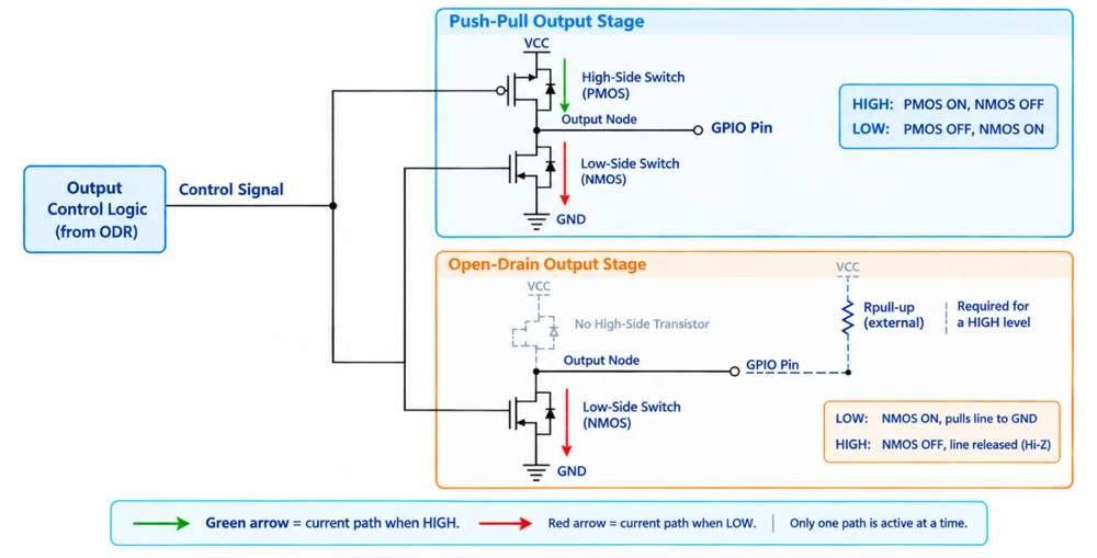
Table of contents
What is a Push-Pull Output?
Push-pull is the default output mode on most GPIO pins, and it is the one most people picture when they think about digital outputs. In this mode, the pin actively drives both logic levels.
|
1 2 |
HIGH → actively drives HIGH LOW → actively drives LOW |
Internally, a push-pull output stage is built from two transistors connected in series between the supply voltage and ground, with the pin connected to the junction between them. One transistor, usually called the high-side switch, connects the pin to VCC. The other, the low-side switch, connects the pin to ground. Only one of the two is turned on at any given time.
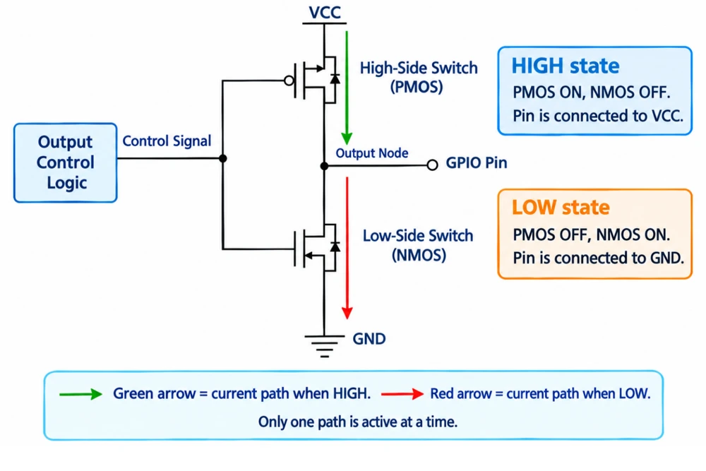
When we write a logic 1 to the pin, the high-side transistor turns on and the low-side transistor turns off. Current flows from the supply, through the high-side switch, out through the pin, and into whatever the pin is connected to. This is what “actively drives HIGH” means: the pin itself is the source of the current that pulls the external line up to VCC.
When we write a logic 0, the situation reverses. The low-side transistor turns on and the high-side transistor turns off. Now the pin connects to ground, and any current flowing into the pin from outside is pulled down to 0V. The pin is “actively driving LOW” in the same sense: it is the low-impedance path that forces the line down.
Because one of the two transistors is always on, a push-pull pin has a low-impedance connection to either VCC or ground at every moment. This gives it strong, fast, symmetric drive in both directions, which is exactly what we want for an LED, a relay driver, or any signal where one microcontroller pin is the sole source of the logic level.
What is an Open-Drain Output?
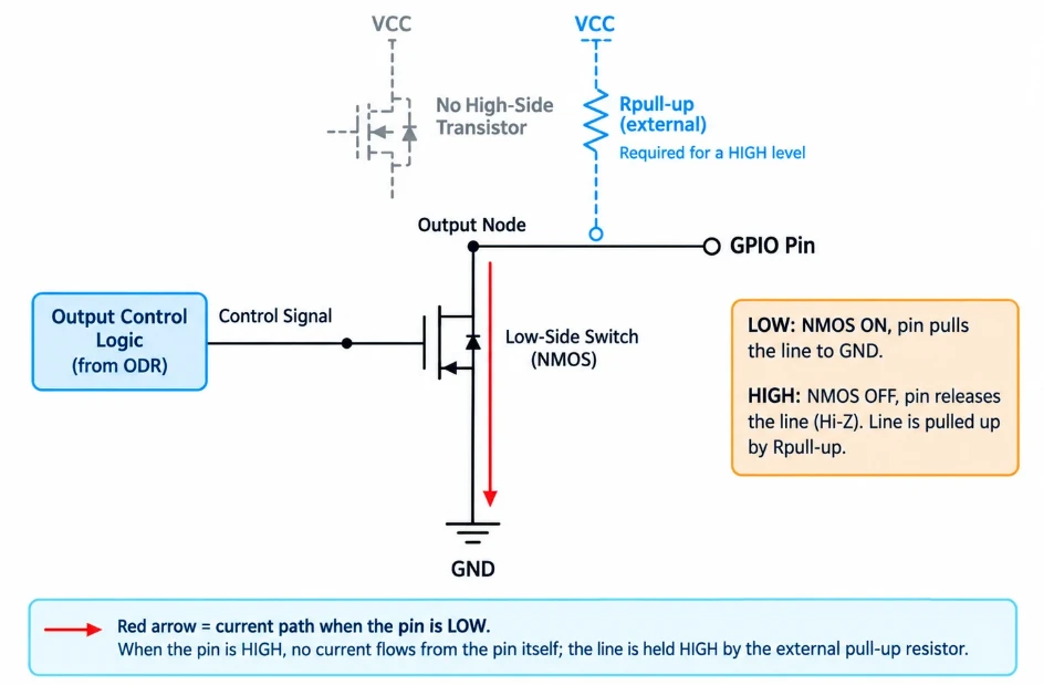
Open-drain works in a different way than push-pull. Instead of two transistors, an open-drain output stage has only one, and it connects the pin to ground.
When we write a logic 0 to an open-drain pin, that single transistor turns on and connects the pin directly to ground, exactly the way the low-side switch does in push-pull mode. The pin actively pulls the line LOW and can sink current the same way it would in push-pull mode.
The difference appears when we write a logic 1. There is no high-side transistor to turn on, so nothing connects the pin to VCC. The transistor simply turns off, and the pin is left disconnected from both ground and the supply. This state is called high-impedance, or Hi-Z. The pin is not setting the line to any particular voltage. It has simply stopped holding it.
|
1 2 |
LOW → actively pulls the line LOW HIGH → releases the line |
This is why the second line above says “releases” rather than “drives HIGH.” The pin itself never puts a HIGH voltage onto the line. Once the pin releases the line, the voltage it settles at depends entirely on whatever else is connected to it, which the next section explains.
Why Does Open-Drain Need a Pull-Up?
An open-drain pin never actively drives the line HIGH, so something else in the circuit has to establish that HIGH level. In almost every real design, that something is an external pull-up resistor connected between the signal line and VCC.
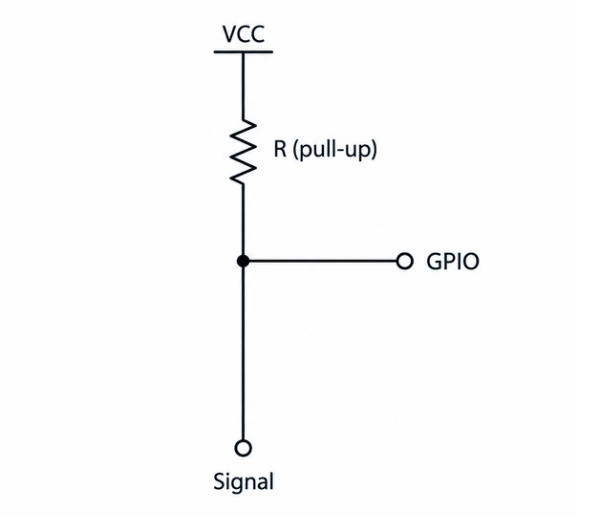
The resistor sits between the supply and the shared signal line. When the open-drain transistor is off, the resistor is the only path left, and it slowly pulls the line up toward VCC. The line settles at a HIGH voltage not because the microcontroller put it there, but because the resistor did. When the open-drain transistor turns on, it overrides the resistor by providing a much lower-resistance path to ground, and the line drops to LOW.
The resistor value matters here. If the value is too large, the line rises slowly, since it is being charged through a high resistance against the parasitic capacitance of the wire and the devices attached to it. This limits how fast the signal can toggle and becomes a real problem at higher communication speeds. If it is too small, it draws more current every time the line is held LOW, since that current now flows from VCC through the resistor and into the transistor holding the line down. Typical pull-up values for I2C lines running at standard or fast mode sit in the 2 kΩ to 10 kΩ range, with the exact figure depending on bus speed, bus capacitance, and how many devices share the line.
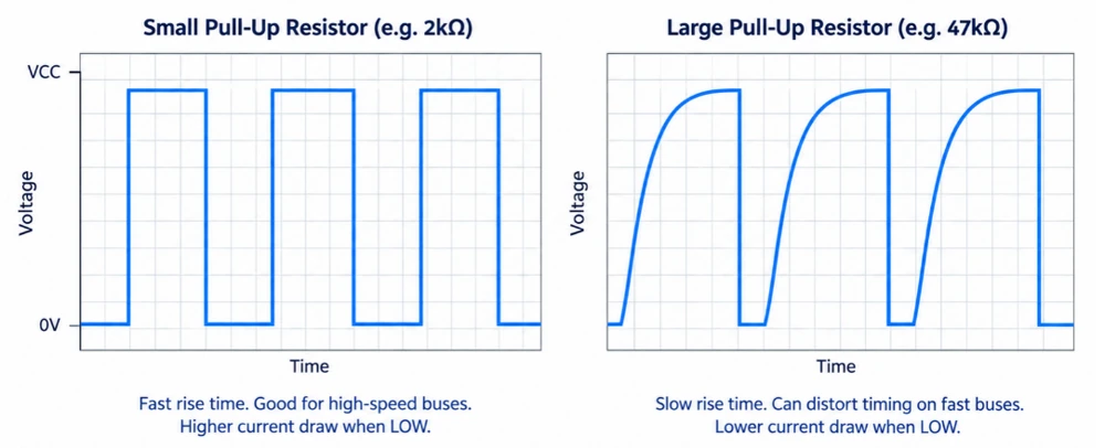
Push-Pull vs Open-Drain Comparison Table
The table below summarizes the practical differences between Push-Pull and Open-Drain covered so far.
| Feature | Push-Pull | Open-Drain |
|---|---|---|
| Drives LOW | Yes | Yes |
| Drives HIGH | Yes | No, requires pull-up |
| External pull-up required | Usually no | Usually yes |
| Shared line | Generally unsuitable | Suitable |
| Typical use | LEDs/control signals | I²C/shared buses |
The row worth a closer look is “Shared line.” Push-pull is a poor fit for any wire that more than one device might drive, because each device forces the line to whatever value it wants through a low-impedance path in both directions. If two push-pull outputs disagree, one is trying to push current toward VCC while the other is trying to pull it toward ground, and neither one has a way to step back. Open-drain avoids this problem by design. A device that wants to stay out of the way simply releases the line instead of fighting over it. This is the property that makes open-drain suitable for shared buses, and it is what the next two sections cover in detail.
What Is Wired-AND in Open-Drain Outputs?
When several open-drain outputs are tied to the same line with a single shared pull-up resistor, the line behaves in a predictable way: it reads LOW if any device on the bus is pulling it LOW, and it only reads HIGH when every device has released it. This behavior is commonly called wired-AND, because the resulting logic level is the logical AND of all the devices’ outputs, using the convention that a released (pulled-up) line represents a 1.
This works safely because of how each device behaves at the transistor level. A device that wants the line LOW, turns on its single transistor and sinks current to ground. A device that wants the line HIGH does nothing at all, it just leaves its transistor off and lets the pull-up resistor handle the job. Since no device ever tries to push current onto the line, there is no case where one device is forcing current out while another is pulling it in. The worst case is simply a device holding the line down against the small current the resistor supplies, and the resistor is sized to handle exactly that.
This is also why the pull-up resistor is shared rather than duplicated per device. One resistor is enough to establish the HIGH level for the whole bus, and adding more pull-ups than necessary just increases the total pull-up current and further slows the rising edge.
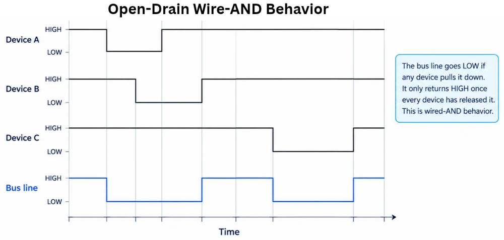
Why Does I2C Use Open-Drain?
I2C is the clearest real-world example of why open-drain exists, so it’s worth working through the electrical reasoning instead of just stating it as a rule.
An I2C bus has two lines, SDA for data and SCL for clock, and both are open-drain with pull-up resistors. Every device on the bus, whether it is currently acting as master or slave, connects to these same two wires. At any point in time, more than one device may need to interact with the same line: a slave pulling SDA LOW to send an acknowledgment bit, a master pulling SCL LOW to stretch the clock while it processes data, or two masters starting a transaction at nearly the same moment during multi-master arbitration.
If SDA and SCL were push-pull, any of these situations could put two devices in direct conflict, each trying to force the line to a different level with a low-impedance connection. Open-drain removes that risk. Every device that wants to release the line just stops driving it, and the pull-up resistor supplies the HIGH level for the whole bus. A device only ever pulls the line down, and pulling down is safe no matter how many other devices are also pulling down at the same time, because of the wired-AND behavior described above.
This is also what makes clock stretching possible. A slow slave device can hold SCL LOW even after the master releases it, delaying the clock until the slave is ready. This only works because SCL is open-drain. The master’s release of the line does not force it HIGH. It simply stops the master from being the one holding it LOW, and the line stays LOW until every device, including the stretching slave, has released it.
Because devices never drive opposite logic levels against each other, an I2C bus can support many devices on the same two wires without any device needing to know in advance whether another device might also try to use the line at that moment.
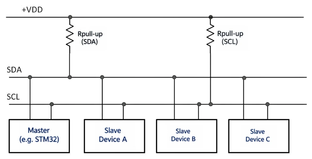
When to Use Push-Pull vs Open-Drain
Neither mode is better in general. Which one to use depends on what the line is connected to and whether more than one device might need to influence it.
Push-pull is the right choice whenever the microcontroller is the sole source of the signal and needs strong, fast drive in both directions. Driving an LED, switching a transistor or MOSFET gate, sending a control signal to a single peripheral, and generating a clock or PWM signal for a dedicated device are all cases where push-pull is the natural fit. There is no ambiguity about who controls the line, so there is no benefit to giving up the active HIGH drive, and doing so would only add an unnecessary resistor and slow the signal down.
Open-drain becomes necessary once you cannot guarantee that your microcontroller is the only thing that might drive that line. Shared communication buses like I2C are the most common case, but the same reasoning applies to a reset line shared between several ICs, a shared interrupt line that any of several peripherals might need to assert, or any signal where you want the option to combine multiple sources safely using wired-AND logic. In all of these cases, the ability to release the line rather than fight over it is the entire point.
A practical way to decide is to ask whether any other device, now or in a future revision of the design, might need to pull that same line to the opposite state your microcontroller is driving. If the answer is no, push-pull is simpler and faster. If the answer is yes, or even might be yes, open-drain with an appropriately sized pull-up is the safer choice.
STM32CubeMX Demo: Push-Pull vs Open-Drain
This demo uses a NUCLEO-F446RE board and configures two pins:
| Pin | Label | Mode | Pull |
|---|---|---|---|
| PA0 | PP_PIN | Output Push Pull | No pull |
| PA1 | OD_PIN | Output Open Drain | Internal pull-up (later changed to no pull) |
Both pins run the same software. The only differences are how each pin is configured and what it does at the transistor level. All you need is a multimeter and two jumper wires. If you are new to STM32CubeMX, read STM32CubeMX Explained first.
Step 1: Set the Pins as Outputs
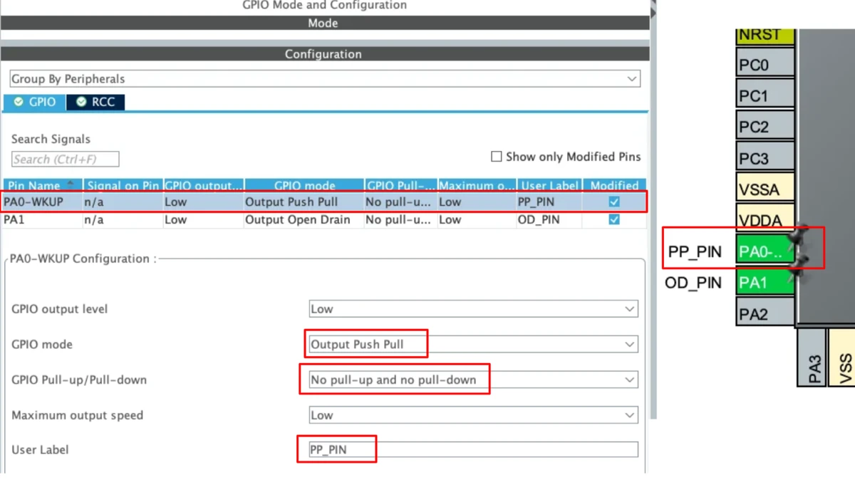
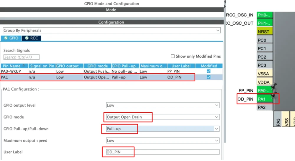
In Pinout & Configuration, click PA0 and choose GPIO_Output. Do the same for PA1.
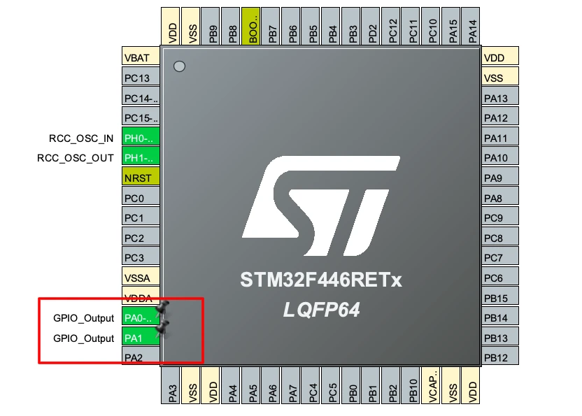
Step 2: Configure the GPIO Settings
Open System Core → GPIO and select each pin in turn.
| Setting | PA0 | PA1 |
|---|---|---|
| GPIO output level | Low | Low |
| GPIO mode | Output Push Pull | Output Open Drain |
| GPIO Pull-up/Pull-down | No pull-up and no pull-down | Pull-up |
| Maximum output speed | Low | Low |
| User Label | PP_PIN | OD_PIN |
Step 3: The Generated Code
CubeMX writes the pin setup into MX_GPIO_Init() in main.c. The exact formatting varies a little between CubeMX versions.
|
1 2 3 4 5 6 7 8 9 10 11 12 13 14 15 16 17 18 19 20 21 22 23 24 25 26 27 28 29 30 31 |
static void MX_GPIO_Init(void) { GPIO_InitTypeDef GPIO_InitStruct = {0}; /* USER CODE BEGIN MX_GPIO_Init_1 */ /* USER CODE END MX_GPIO_Init_1 */ /* GPIO Ports Clock Enable */ __HAL_RCC_GPIOA_CLK_ENABLE(); /*Configure GPIO pin Output Level */ HAL_GPIO_WritePin(GPIOA, PP_PIN_Pin|OD_PIN_Pin, GPIO_PIN_RESET); /*Configure GPIO pin : PP_PIN_Pin */ GPIO_InitStruct.Pin = PP_PIN_Pin; GPIO_InitStruct.Mode = GPIO_MODE_OUTPUT_PP; GPIO_InitStruct.Pull = GPIO_NOPULL; GPIO_InitStruct.Speed = GPIO_SPEED_FREQ_LOW; HAL_GPIO_Init(PP_PIN_GPIO_Port, &GPIO_InitStruct); /*Configure GPIO pin : OD_PIN_Pin */ GPIO_InitStruct.Pin = OD_PIN_Pin; GPIO_InitStruct.Mode = GPIO_MODE_OUTPUT_OD; GPIO_InitStruct.Pull = GPIO_PULLUP; GPIO_InitStruct.Speed = GPIO_SPEED_FREQ_LOW; HAL_GPIO_Init(OD_PIN_GPIO_Port, &GPIO_InitStruct); /* USER CODE BEGIN MX_GPIO_Init_2 */ /* USER CODE END MX_GPIO_Init_2 */ } |
The names PP_PIN_Pin and OD_PIN_GPIO_Port come from the user labels, and CubeMX defines them in main.h. If we compare the two blocks, the only differences are Mode ( GPIO_MODE_OUTPUT_PP vs GPIO_MODE_OUTPUT_OD) and Pull ( GPIO_NOPULL vs GPIO_PULLUP).
Step 4: Add the Application Code
In main.c, add a hold-time define between the private-define markers:
|
1 2 3 |
/* USER CODE BEGIN PD */ #define HOLD_TIME_MS 3000 // long enough to read a multimeter /* USER CODE END PD */ |
Then add the loop body between the USER CODE BEGIN 3 markers:
|
1 2 3 4 5 6 7 8 9 10 11 12 13 14 15 |
while (1) { /* USER CODE END WHILE */ /* USER CODE BEGIN 3 */ // Write HIGH to both pins HAL_GPIO_WritePin(PP_PIN_GPIO_Port, PP_PIN_Pin, GPIO_PIN_SET); HAL_GPIO_WritePin(OD_PIN_GPIO_Port, OD_PIN_Pin, GPIO_PIN_SET); HAL_Delay(HOLD_TIME_MS); // Write LOW to both pins HAL_GPIO_WritePin(PP_PIN_GPIO_Port, PP_PIN_Pin, GPIO_PIN_RESET); HAL_GPIO_WritePin(OD_PIN_GPIO_Port, OD_PIN_Pin, GPIO_PIN_RESET); HAL_Delay(HOLD_TIME_MS); } |
Both pins receive identical writes. Keep all custom code between the USER CODE markers, or CubeMX will delete it when you regenerate the project.
Step 5: Wiring
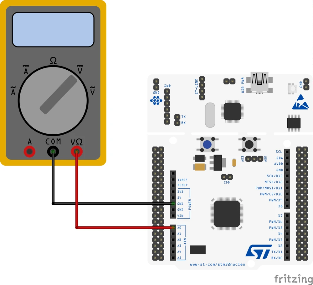
Connect the multimeter to the Nucleo’s Arduino header:
- Black probe: any GND pin on the header
- Red probe: A0 (PA0) for the push-pull test, A1 (PA1) for the open-drain test
Step 6: Build, Flash, and Measure
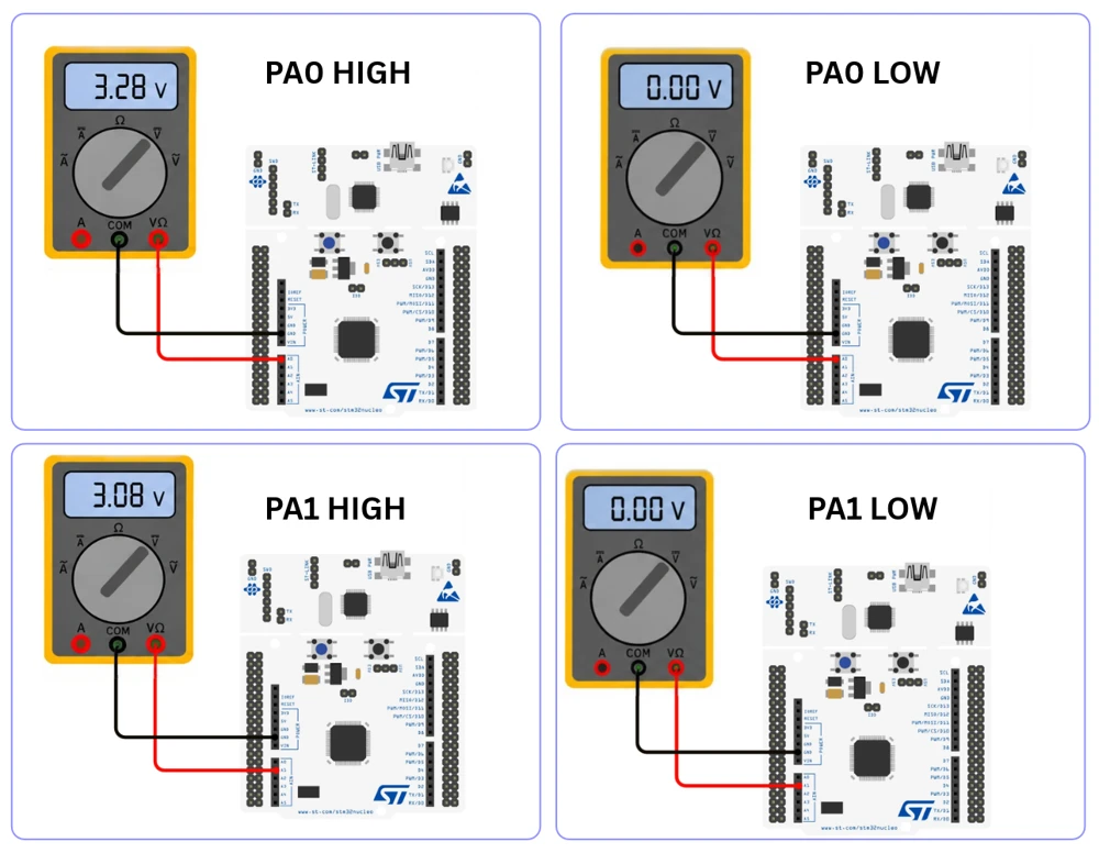
Click Build, then Run. Each level holds for three seconds, so you can read the meter in each state.
- PA0 (push-pull) HIGH. Expect close to 3.3 V. The pin’s own high-side transistor drives the level.
- PA0 LOW. Expect close to 0 V.
- PA1 (open-drain, internal pull-up) HIGH. Expect close to 3.3 V. The pin has released the line and the internal pull-up supplies the HIGH level. A multimeter draws almost no current, so it doesn’t reveal how weak the pull-up is.
- PA1 LOW. Expect close to 0 V. The open-drain transistor actively pulls the line down.
Step 7: Remove the Pull-Up
Now the control test. In CubeMX, select PA1 and set GPIO Pull-up/Pull-down to No pull-up and no pull-down.
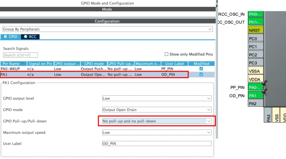
After regenerating the project, only 1 line changes. Build and flash this project again.
|
1 |
GPIO_InitStruct.Pull = GPIO_NOPULL; // was GPIO_PULLUP |
Measure PA1 again:
- PA1 HIGH. The reading becomes unstable or drifts, and may settle at an arbitrary value depending on noise and probe loading. The pin has released the line and nothing holds it up.
- PA1 LOW. Still close to 0 V, since the open-drain pin can pull LOW without any help.
This is why the pull-up is essential. The software is identical to the last run, and only the pin’s electrical setup changed.
What We Learned From the Measurements
The software was identical in every test: both pins were written HIGH and LOW with HAL_GPIO_WritePin(). Only the pin configuration changed, and the readings changed with it.
- Push-pull (PA0) held about 3.28 V when HIGH and about 0 V when LOW. The pin’s own transistors drive both levels.
- Open-drain with internal pull-up (PA1) read about 3.08 V when HIGH and about 0 V when LOW. The pull-up supplies the HIGH level, and the pin only pulls the line down.
- Open-drain with no pull (PA1) gave an unstable reading when HIGH, because nothing holds the line up once the pin lets go. LOW was still about 0 V.
The 0.2 V gap between PA0 and PA1 when HIGH shows that the internal pull-up is weak. Even a multimeter draws enough current to pull it down a little, so real buses like I²C use external pull-ups of a few kΩ.
What the Edges Look Like
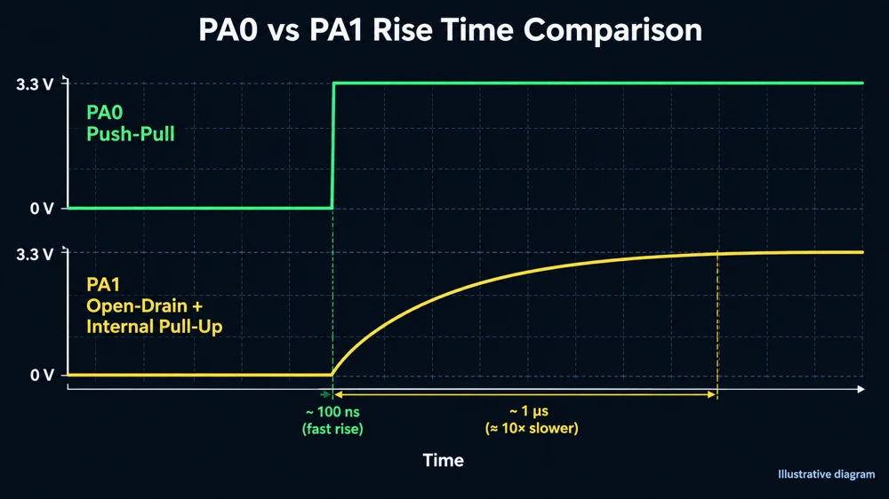
An oscilloscope shows the biggest difference between the two modes, which is speed. The push-pull pin has its own transistor charging the line, so its rising edge is sharp. The open-drain pin has to charge the wiring capacitance through a pull-up of tens of kΩ, so its edge follows a slow RC curve. As a rough estimate with a 40 kΩ pull-up and about 20 pF of load, the 10-to-90% rise time is about 2.2 × R × C ≈ 1.8 µs, roughly ten times slower than with a 4.7 kΩ external pull-up.
Results
| Configuration | HIGH reading | LOW reading | Observation |
|---|---|---|---|
| PA0, push-pull | 3.28 V | 0 V | Drives both levels |
| PA1, open-drain + internal pull-up | 3.08 V | 0 V | HIGH supplied by pull-up, slightly loaded by the meter |
| PA1, open-drain, no pull | (unstable) | 0 V | HIGH floats |
Wrapping Up
Push-pull and open-drain describe two different ways an STM32 pin can drive a line once it is set up as an output. Push-pull uses a pair of transistors to actively drive both HIGH and LOW, which gives it strong, symmetric drive suited to signals with a single source, such as an LED or a control line to one peripheral. Open-drain uses a single transistor to actively pull the line LOW and relies on an external pull-up resistor to establish the HIGH level, which makes it the right choice whenever more than one device might need to influence the same line.
That difference is exactly why I2C, and other shared buses like it, depend on open-drain outputs. Every device on the bus can pull the line LOW without risking a conflict with any other device, and the pull-up resistor quietly does the job of restoring the HIGH level once every device has released the line. Understanding this at the transistor level makes the rest of I2C, from clock stretching to multi-master arbitration, much easier to reason about, and it makes the difference between a bus that works reliably and one that produces mysterious, intermittent errors on the bench.
Download the Project Here
Download the CubeMX project files and HAL source code — all tested on real hardware.
If you find this useful, you can support us with a Donation as well.