STM32 Alternate Function Pins Explained
Every pin of an STM32 microcontroller has a name such as PA9, PB0, PC13, etc. This name only identifies the position of the pin in the respective GPIO port. It does not decide what the pin does. The same physical pin can be driven by the GPIO registers, by a UART transmitter, or by a timer output, depending on how the device is configured. Many users meet this idea for the first time when a UART or PWM signal does not appear on the pin they expected. In most of these cases, the cause is a wrong alternate function setting.
In this article, we will understand how alternate functions connect peripherals to physical pins. We will begin with the definition of an alternate function and the reason why pins have several functions. Then we will compare GPIO mode with alternate function mode. After that, we will look at the internal pin multiplexer, the alternate function numbers, and the way STM32CubeMX selects them, followed by examples with UART, timer, and SPI signals. In the later sections, we will learn to read the alternate function table in the datasheet and go through the common mistakes.
This article is part of the STM32 GPIO tutorial series.
Table of contents
- STM32 Alternate Function Pins Explained
What is an Alternate Function?
Inside an STM32 device, peripherals such as the USART, SPI, and the timers are separate hardware blocks. Each block exchanges signals with the outside world. For example, the transmit line of a UART, the clock line of an SPI bus, and the output channel of a timer. These signals begin as internal wires that can reach another device only through a physical pin of the package.
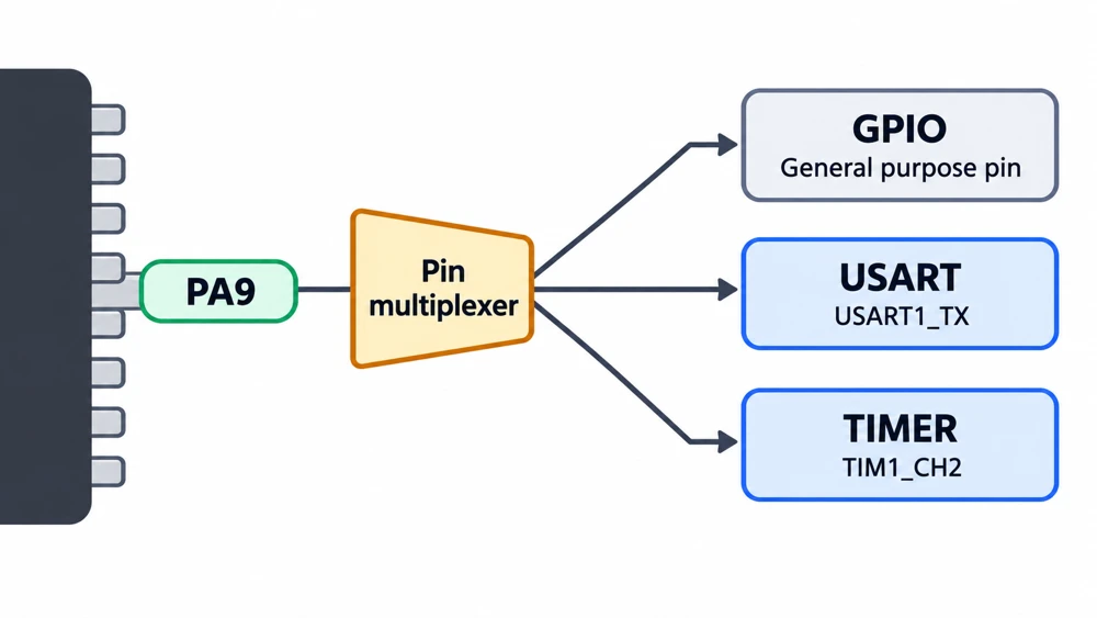
An alternate function is the mode in which a pin is handed over from the GPIO block to one of these peripherals. In simple terms, a peripheral can control a physical pin through the microcontroller’s internal pin multiplexing system. The word alternate is used because the default role of the pin is general purpose I/O. The peripheral signal is an alternative to that role. The diagram below shows this for the pin PA9.
The pin is connected to only one of the three owners at a time. The choice is stored in the GPIO port registers. The multiplexer routes the selected signal to the pin and keeps the others disconnected.
Peripheral Signal Names
Signal names follow a pattern that is easy to read once the pattern is known. The first part names the peripheral instance, and the second part names the signal. For example, USART1_TX is the transmit output of the first USART, TIM1_CH1 is the first channel of timer 1, and SPI1_SCK is the clock line of the first SPI peripheral. The same names appear in the datasheet, in the CubeMX pinout view, and in HAL constants such as GPIO_AF7_USART1.
Why STM32 Pins Have Multiple Functions
A modern STM32 device contains a large number of peripherals. The STM32F446, for example, has six USART and UART blocks, three SPI blocks, three I²C blocks, and a large group of timers. It also has interfaces such as CAN, SAI, and USB. Together these blocks expose over a hundred external signals. The 64-pin package used on the NUCLEO-F446RE board offers only about 50 pins that can be used for I/O.
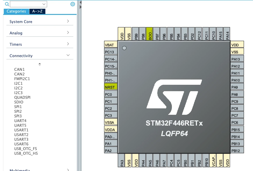
If every signal is given its own dedicated pin, we would need a package with hundreds of pins. This would raise the cost of the chip, the area of the board, and the complexity of the PCB. Therefore manufacturers share each pin between several signals and let the user decide which one is connected. This is the reason why a single pin such as PA9 appears in the datasheet with a GPIO function, a USART function, a timer function, and others.
GPIO Mode vs Alternate Function Mode
The difference between the two modes lies in the block that controls the pin.
In GPIO mode, the GPIO peripheral controls the pin. Software writes to the output data register or to the BSRR register, and the output driver follows that value.
In alternate function mode, the GPIO block steps aside, and the output data register is disconnected from the driver. The signal coming from the selected peripheral drives the pin instead. Software only controls the pin indirectly, by configuring the peripheral and writing to its registers.
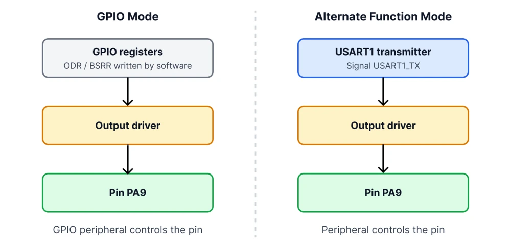
The mode of each pin is stored in a two-bit field of the mode register. This register is called GPIOx_MODER on the STM32F4 series. The four possible values are listed in the table below, together with the HAL constants that CubeMX generates for them.
| MODER value | Pin mode | HAL constant |
|---|---|---|
| 00 | Input | GPIO_MODE_INPUT |
| 01 | General purpose output | GPIO_MODE_OUTPUT_PP, GPIO_MODE_OUTPUT_OD |
| 10 | Alternate function | GPIO_MODE_AF_PP, GPIO_MODE_AF_OD |
| 11 | Analog | GPIO_MODE_ANALOG |
The mode selection is only one part of the configuration. A pin in alternate function mode still has an output type, a pull setting, and a speed setting. This is because the same output driver is used in both modes. HAL therefore offers two alternate function modes, GPIO_MODE_AF_PP for push-pull and GPIO_MODE_AF_OD for open-drain.
A UART transmitter or an SPI clock normally uses push-pull. The I²C lines use open-drain with an external pull-up resistor, as described in the push-pull vs open-drain article. The speed setting from the previous article also applies here. A fast SPI clock needs steeper edges than a slow UART line.
STM32 Pin Multiplexing
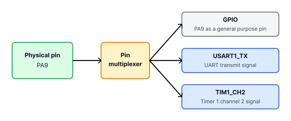
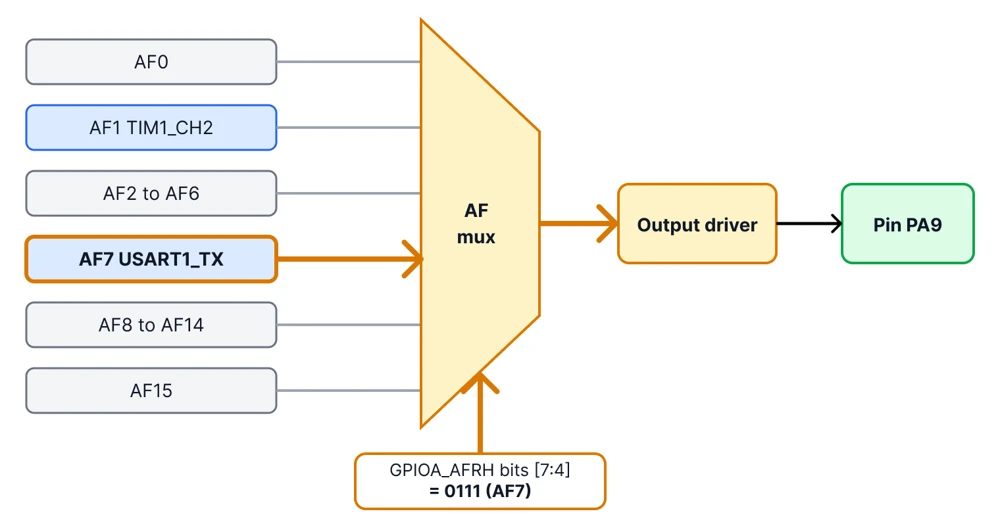
A multiplexer is a circuit with several inputs and a single output. A selection input decides which of the inputs reaches the output. Each STM32 pin has a multiplexer of this kind in front of its output driver, with one input for every peripheral signal that can use the pin. The selection is stored in alternate function registers of the GPIO port. The diagram below shows the multiplexer of PA9 in a simplified form.
The AFR Registers
On the STM32F4 series, every pin has a four-bit field in one of two alternate function registers. GPIOx_AFRL holds the fields of pins 0 to 7. GPIOx_AFRH holds the fields of pins 8 to 15. Four bits can store sixteen values, which are called AF0 to AF15. Each value corresponds to one input of the multiplexer. For PA9, pin 9 is the second field of the high register at bits 7:4, and the value 7 selects USART1_TX.
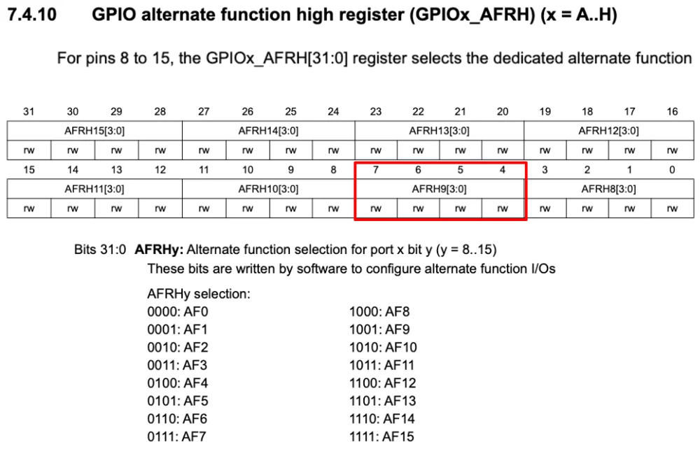
The two settings therefore work together on every pin. The mode field in GPIOx_MODER decides whether the pin belongs to the GPIO block or to the peripherals. The field in the AFR register decides which peripheral signal is used. If the mode is not set to alternate function, the AFR value has no effect on the pin. If the mode is set correctly but the AF number is wrong, a different peripheral signal reaches the pin. In some cases the pin receives a signal from a peripheral that is not active.
Only one signal can control a pin at a given moment, because the multiplexer has a single selection. Two peripherals cannot share one pin at the same time. The firmware is free to change the selection while the program runs.
Alternate Function Numbers
The alternate function number is the value that is written into the AFR field of a pin. On the STM32F4 series, the numbers run from AF0 to AF15. The table below shows how the numbers are typically grouped on this series. It is meant as an orientation and not as a reference. The exact content of each column depends on the device.
| AF number | Typical peripherals on STM32F4 |
|---|---|
| AF0 | System functions such as SWD, JTAG, trace, and the MCO clock output |
| AF1 | TIM1, TIM2 |
| AF2 | TIM3, TIM4, TIM5 |
| AF3 | TIM8, TIM9, TIM10, TIM11 |
| AF4 | I²C1, I²C2, I²C3, I²C4 |
| AF5 | SPI1, SPI2, SPI3, SPI4 |
| AF6 | SPI2, SPI3, SPI4 and SAI on some pins |
| AF7 | USART1, USART2, USART3, UART5, SPDIF |
| AF8 | USART1, USART2, USART3, UART5, SPDIF |
| AF9 | CAN1, CAN2, TIM12, TIM13, TIM14, QUADSPI |
| AF10 to AF14 | USB, memory interfaces, camera interface, and other device-specific blocks |
| AF15 | EVENTOUT |
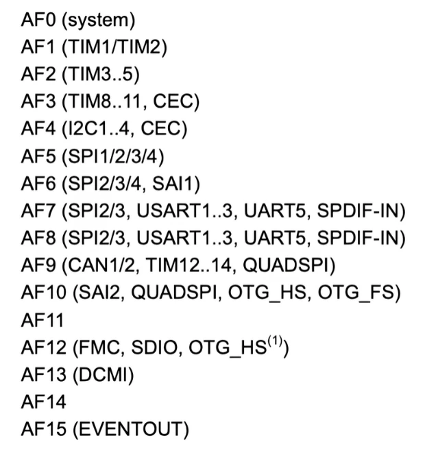
The alternate function mappings are specific to the MCU family and to the individual device. The STM32F1 series, for example, has no AFR registers at all. It moves peripheral signals between pins with a separate remap mechanism in the AFIO block. Newer families such as the STM32G4 and STM32L4 use the same AF0 to AF15 scheme as the STM32F4, but many of the assignments are different. Even within one device, a signal does not always use the same AF number on every pin where it appears. Therefor the number has to be read for the exact pin and the exact device.
CubeMX Alternate Function Setup
STM32CubeMX hides the lookup of AF numbers from the user, and the process follows the same steps every time. The user first enables a peripheral and then selects a pin for each of its signals. CubeMX then looks up the matching AF number for that pin. It writes the result into the generated GPIO configuration.
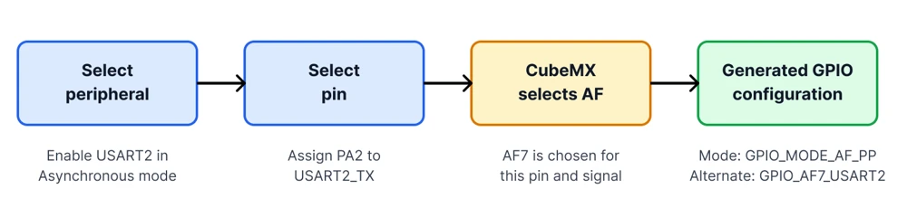
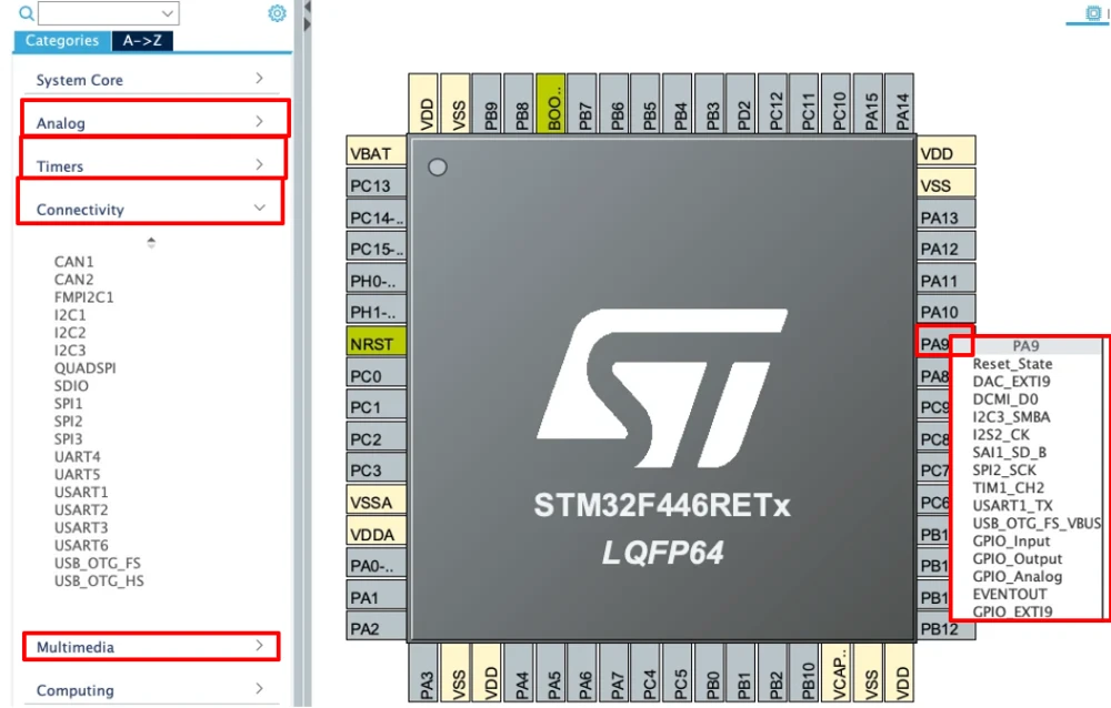
In the Pinout & Configuration tab, the pin list on the left shows the peripherals. A mode such as Asynchronous for a USART makes CubeMX assign default pins to its signals. Whereas, clicking a pin in the chip view opens a drop-down list. This list contains only the functions the pin can carry on the selected device, so an invalid combination cannot be chosen by mistake. Holding the Ctrl key while clicking a pin highlights the other pins that can carry the same signal. This makes it easy to move a signal to a different location. If two peripherals request the same pin, CubeMX marks the conflict in the pinout view.
The generated code of a peripheral pin is placed in the MSP initialization function of that peripheral in stm32f4xx_hal_msp.c. The AF number appears in the Alternate field of the GPIO_InitTypeDef structure, as shown in the example at the end of this article.
UART, Timer PWM and SPI Examples
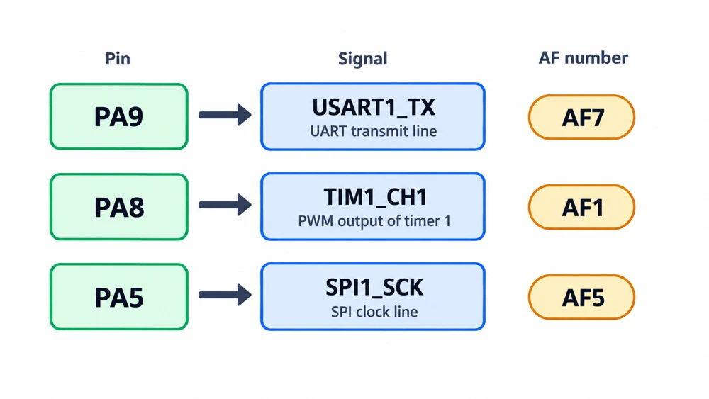
The three most common uses of alternate functions are serial communication, PWM output, and SPI communication. The table below lists one pin for each of them. The pins mentioned are for the STM32F446, and the AF numbers follow the datasheet of this device. You must check the datasheet of the exact MCU before using it in a design.
| Pin | Signal | AF number | HAL constant | Peripheral use |
|---|---|---|---|---|
| PA9 | USART1_TX | AF7 | GPIO_AF7_USART1 | UART transmit line |
| PA8 | TIM1_CH1 | AF1 | GPIO_AF1_TIM1 | PWM output of timer 1 |
| PA5 | SPI1_SCK | AF5 | GPIO_AF5_SPI1 | SPI clock line |
Each of these pins has other functions as well. PA9 can also carry TIM1_CH2 with AF1, and PA5 can carry TIM2_CH1 with AF1. The choice of the AF number therefore decides which of these functions actually reaches the pin.
In all three cases, the pin is configured as an alternate function pin. The UART also needs its receive pin on PA10 with the same AF7. The SPI bus needs its data pins PA6 and PA7 with AF5 as well. We must configure every signal of the peripheral being used. A missing configuration on any one of these pins breaks the connection.
Alternate Functions in the Datasheet
Reading the alternate function table is an important practical skill. It gives the final answer for every pin and every AF number, independent of the tool that generated the project. The datasheet of the device contains two tables that serve this purpose. Each table answers a different question.
The Pin Definitions Table
The pin definitions table has one row per pin. It lists the pin number in each package, the pin name, the pin type, and the I/O structure. After that come two columns for functions. The alternate functions column lists every signal that the pin can carry in alternate function mode. The additional functions column lists the analog and special functions, such as ADC inputs and the oscillator pins.
This table is the first place to look when a pin has to be chosen for a board. It shows whether the pin exists in the package and which signals it offers. However, it does not show the AF number of each signal.
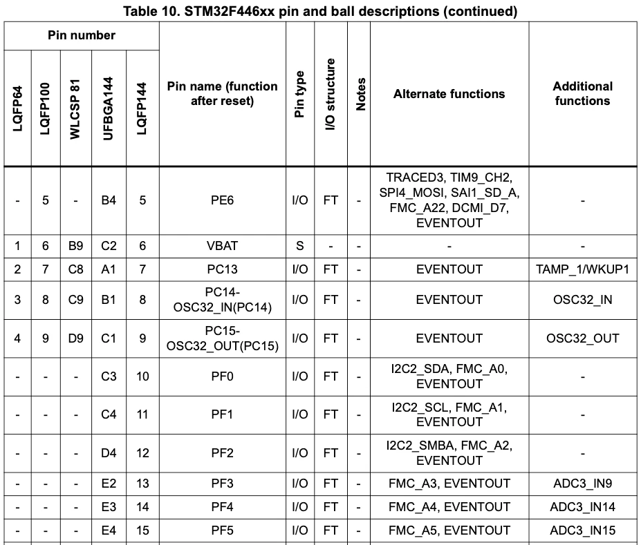
The Alternate Function Table
The alternate function mapping table has one row per port pin and one column per AF number, from AF0 to AF15. Each cell contains the signal that is selected when the column number is written into the AFR field of that pin. An empty cell means that the AF number is not used on this pin. The table snippet below shows a simplified version of three rows, with only the columns that are needed for this article.
| Port pin | AF0 | AF1 | AF7 |
|---|---|---|---|
| PA8 | MCO1 | TIM1_CH1 | USART1_CK |
| PA9 | TIM1_CH2 | USART1_TX | |
| PA10 | TIM1_CH3 | USART1_RX |
To use the table, start with the row of the pin. Move along the row until the required signal is found, and then read the header of that column. For USART1_TX on PA9, the signal is found in the AF7 column. The value 7 is therefore the one that goes into the AFR field, and the HAL constant is GPIO_AF7_USART1. The table is also a good source for understanding the conflicts of a pin. Every signal in the same row is a function that cannot be used at the same time as the selected one.
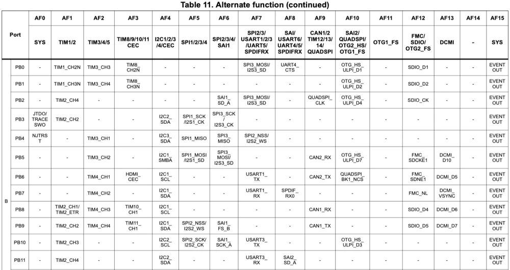
Searching from the Signal
The lookup also works in the opposite direction. When the signal is known and the pin is not, a text search for the signal name in the PDF, for example USART1_TX, lists every cell in which it appears. Each result shows one possible pin together with its AF number. This makes it easy to compare the options and to choose a pin that fits the board layout and is not used by another function.
STM32 Alternate Function Example
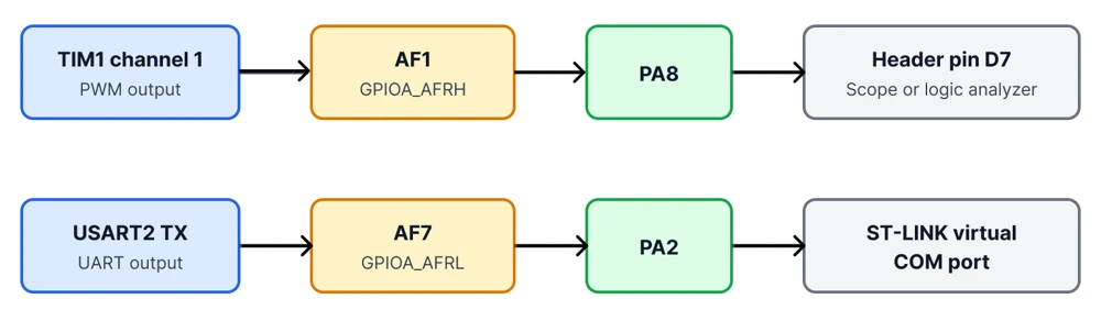
This example uses two alternate functions on a NUCLEO-F446RE board at the same time. Timer 1 channel 1 creates a 1 kHz PWM signal with a 25 percent duty cycle on pin PA8. USART2 sends a text message once per second using pin PA2. The first signal is output on the Arduino header pin D7 and can be observed with an oscilloscope or a logic analyzer. The second signal passes through the ST-LINK virtual COM port, so it appears in a serial terminal on the PC without extra wiring. The two pins use different AF numbers, AF1 for the timer and AF7 for the UART. The diagram below shows how both signals reach their pins.
Step 1: Configure the Timer
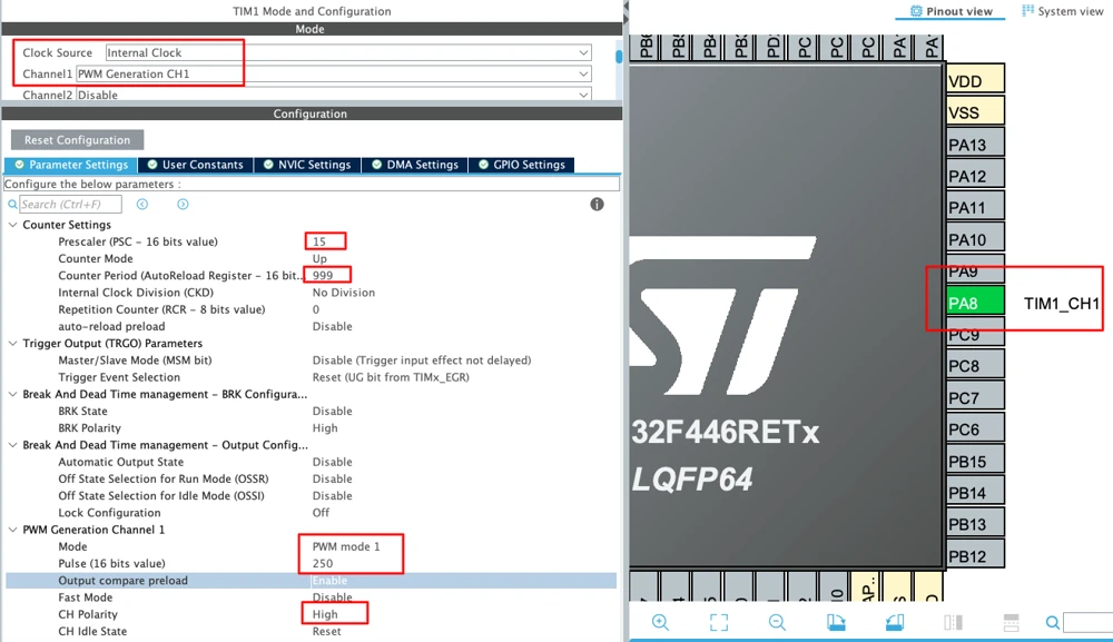
In the Pinout & Configuration tab, open Timers → TIM1 and set Clock Source to Internal Clock. Then set Channel1 to PWM Generation CH1. CubeMX assigns the signal to PA8 automatically, and the pin turns green in the chip view. Enter the parameters from the table below.
| Setting | Value |
|---|---|
| Prescaler (PSC) | 15 |
| Counter Period (ARR) | 999 |
| Pulse (CCR) | 250 |
| PWM Mode | PWM mode 1 |
| CH Polarity | High |
These values give a PWM frequency of 1 kHz with a 25 percent duty cycle when the timer clock is 16 MHz. This is the case when the clock tree of the project is left at its default HSI setting. If the clock configuration is changed, the frequency changes in the same proportion. The actual timer clock can be read in the Clock Configuration tab.
Step 2: Configure the UART
Open Connectivity → USART2 and set the mode to Asynchronous. On the NUCLEO-F446RE, the pins PA2 and PA3 are connected to the ST-LINK virtual COM port. Use the parameters from the table below.
| Setting | Value |
|---|---|
| Baud Rate | 115200 Bits/s |
| Word Length | 8 Bits |
| Parity | None |
| Stop Bits | 1 |
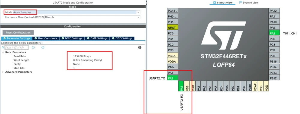
After both peripherals are configured, the pinout view shows PA8 as TIM1_CH1, PA2 as USART2_TX, and PA3 as USART2_RX.
Step 3: The Generated Code
CubeMX writes the pin configuration of each peripheral into stm32f4xx_hal_msp.c. The timer pin is configured in HAL_TIM_MspPostInit(). The UART pins are configured in HAL_UART_MspInit(). The excerpts below show only the lines that matter for this article.
|
1 2 3 4 5 6 7 8 9 10 11 12 13 14 15 16 17 18 19 20 21 |
/**TIM1 GPIO Configuration PA8 ------> TIM1_CH1 */ GPIO_InitStruct.Pin = GPIO_PIN_8; GPIO_InitStruct.Mode = GPIO_MODE_AF_PP; GPIO_InitStruct.Pull = GPIO_NOPULL; GPIO_InitStruct.Speed = GPIO_SPEED_FREQ_LOW; GPIO_InitStruct.Alternate = GPIO_AF1_TIM1; HAL_GPIO_Init(GPIOA, &GPIO_InitStruct); /**USART2 GPIO Configuration PA2 ------> USART2_TX PA3 ------> USART2_RX */ GPIO_InitStruct.Pin = GPIO_PIN_2|GPIO_PIN_3; GPIO_InitStruct.Mode = GPIO_MODE_AF_PP; GPIO_InitStruct.Pull = GPIO_NOPULL; GPIO_InitStruct.Speed = GPIO_SPEED_FREQ_VERY_HIGH; GPIO_InitStruct.Alternate = GPIO_AF7_USART2; HAL_GPIO_Init(GPIOA, &GPIO_InitStruct); |
Both blocks use GPIO_MODE_AF_PP. The only difference between them is the Alternate field, which is GPIO_AF1_TIM1 for the timer and GPIO_AF7_USART2 for the UART. This one field is what connects each pin to its own peripheral.
Step 4: Add the Application Code
We need to start the PWM output once before the main while loop and then send the UART messages inside the loop. Add the code between the USER CODE markers so that CubeMX keeps it when the project is regenerated.
|
1 2 3 4 5 6 7 8 9 10 11 12 13 14 15 16 17 |
/* USER CODE BEGIN 2 */ HAL_TIM_PWM_Start(&htim1, TIM_CHANNEL_1); /* USER CODE END 2 */ /* Infinite loop */ /* USER CODE BEGIN WHILE */ while (1) { /* USER CODE END WHILE */ /* USER CODE BEGIN 3 */ const char data[] = "PA2 is transmitting through USART2\r\n"; HAL_UART_Transmit(&huart2, (uint8_t *)data, sizeof(data) - 1, HAL_MAX_DELAY); HAL_Delay(1000); } |
The function HAL_TIM_PWM_Start() enables the channel and the main output of the timer TIM1. After that call, the timer runs in hardware. The CPU is free to handle the UART transmission.
Step 5: Result
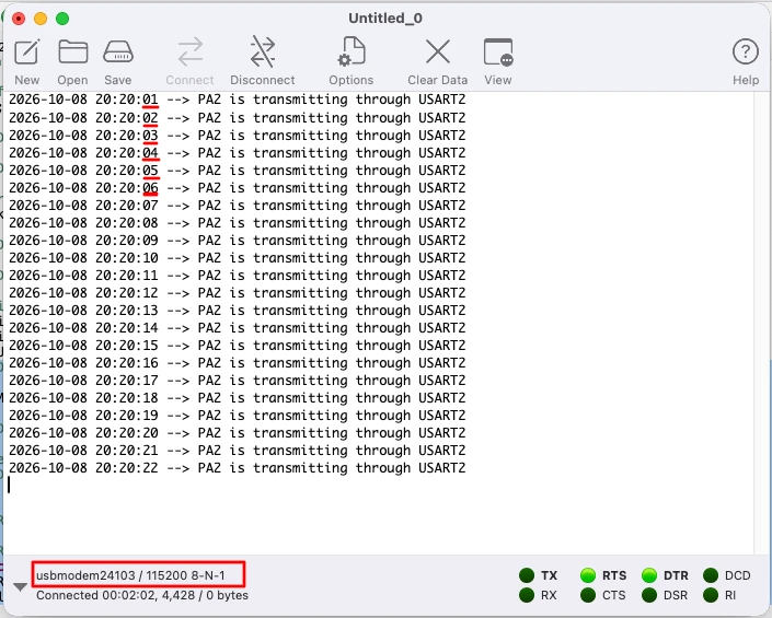
After flashing the project, open a serial terminal on the virtual COM port of the board with 115200 baud, 8 data bits, no parity, and 1 stop bit. The terminal shows the message once per second.
At the same time, a scope or a logic analyzer connected to the header pin D7 shows a 1 kHz square wave. The signal is high for 25 percent of each period.

Conclusion
An alternate function is the mechanism that allows a peripheral to control a physical pin instead of the GPIO block. Each pin contains a multiplexer, and the two settings control it. The mode field in the MODER register decides whether the pin belongs to the GPIO block or to the peripherals. The four-bit field in the AFR registers selects which peripheral signals reaches the pin. Only one signal can control a pin at a time. This sharing is how a package with a limited number of pins can offer a large number of peripheral signals.
The AF numbers are specific to the MCU family and to the individual device. They should always be taken from the datasheet of the selected microcontroller, either by reading the alternate function table directly or by letting CubeMX select them. Most of the problems in practice come from a small number of causes. These are a wrong pin or AF number, a peripheral that has not been started, a pin that was left in normal output mode, a conflict with another function on the board, and a signal that is not available in the package.
Download the Project Here
Download the CubeMX project files and HAL source code — all tested on real hardware.
If you find this useful, you can support us with a Donation as well.