STM32 GPIO Registers Explained
Every call to a HAL GPIO function ends in a read or a write of a hardware register. These registers are ordinary 32-bit locations in the memory map of the microcontroller, and each of them is connected directly to the GPIO hardware. A write to one of these locations changes the electrical state of a pin. We generally do not see this layer, because CubeMX and HAL hide it behind function names and configuration structures. This works well until a pin does not behave as expected, and the only way to find the cause is to look at the registers.
In this article, we will understand how STM32 GPIO registers work underneath HAL. We will begin with the reasons for learning the registers and the way the GPIO register block is organized. Then we will go through the four configuration registers, the two data registers, the BSRR register, and the alternate function registers. After that, we will see how all of them work together on one pin and how a HAL call compares with its register-level equivalent. In the later sections, we will cover a working example that controls an LED on the NUCLEO-F446RE board without HAL.
The examples in this article use the STM32F4 series and the device header stm32f4xx.h. This article is part of the STM32 GPIO tutorial series.
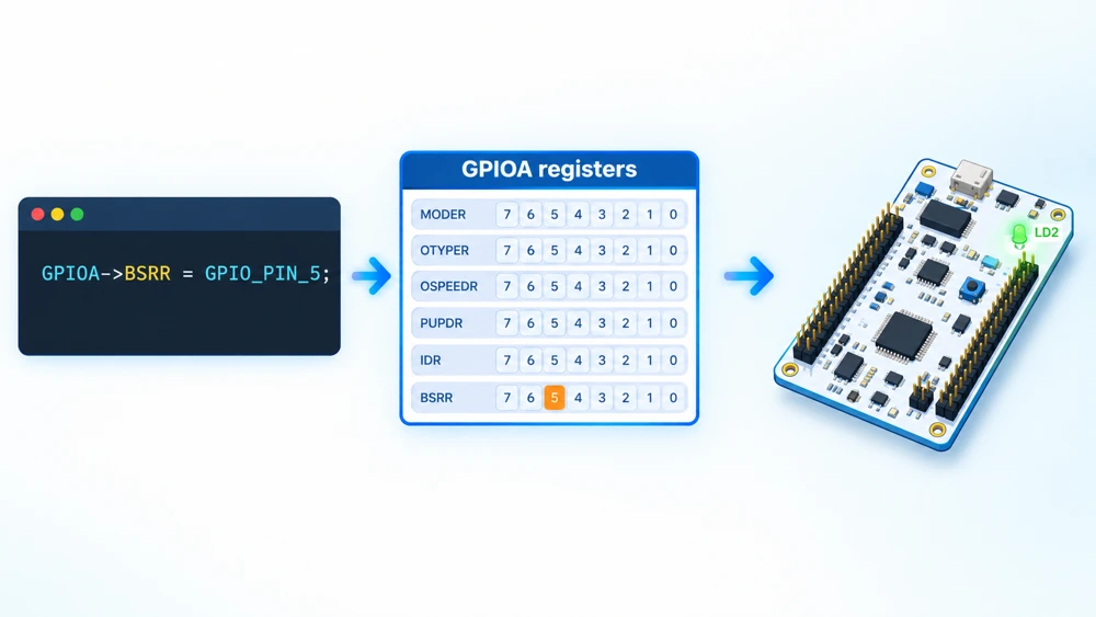
Table of contents
Why Learn GPIO Registers
HAL is a layer of C code that sits between the application and the hardware. It is useful because the same function call works on many STM32 families. The layer does not change the way the hardware works, and every HAL function eventually performs the same register accesses that we can write by hand. The diagram below shows the path from a HAL call to the physical pin.
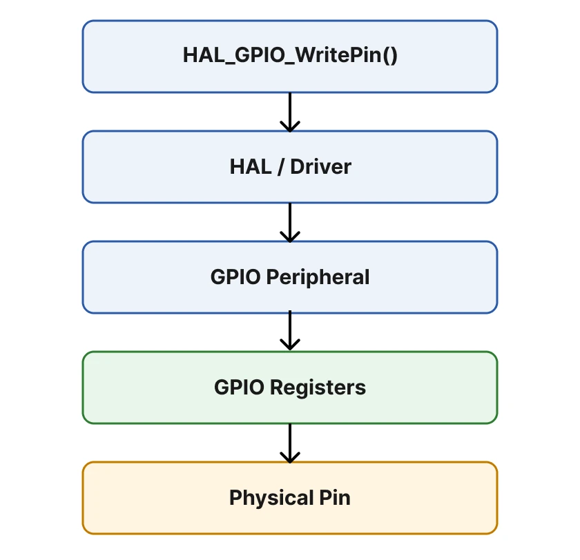
The first benefit of knowing the registers is understanding what HAL does. A function such as HAL_GPIO_Init() looks like a single operation, but it writes to several configuration registers for every pin. Once these registers are known, each field of the GPIO_InitTypeDef structure can be linked to the bits that it changes.
The second benefit is debugging. The debugger of STM32CubeIDE can show the registers of every peripheral in its SFRs view. When a pin does not toggle, a comparison of the register values with the expected values shows whether the problem lies in the mode, the output type, the alternate function, or the port clock. This is often faster than reading the source code of a driver.
The third benefit is the ability to read the reference manual. The manual describes every peripheral through its registers, so the skill of reading a register description is needed for every peripheral and not only for GPIO. GPIO is the simplest peripheral of the device, which makes it a good place to learn this skill. The same ideas of memory-mapped registers, bit fields, and masks also apply to every other microcontroller, and they form a part of the fundamentals of embedded systems.
GPIO Register Structure
Each GPIO port is a separate peripheral with its own block of registers. On the STM32F4 series, every block contains ten 32-bit registers, and the blocks of neighbouring ports are placed 0x400 bytes apart. GPIOA starts at the address 0x40020000, GPIOB starts at 0x40020400, and the other ports follow in the same way. Because the registers are memory mapped, the CPU accesses them like ordinary variables. A write to the address 0x40020014 therefore changes the output data register of GPIOA.
The CMSIS device header describes each block as a C structure called GPIO_TypeDef and defines the names GPIOA, GPIOB, and so on as pointers to the base addresses. This is the reason why we can write GPIOA->ODR in the source code. The diagram below shows the registers of one port with their offsets.
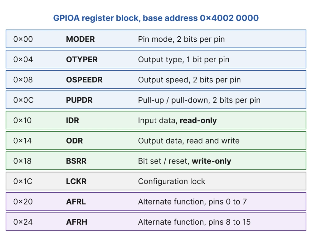
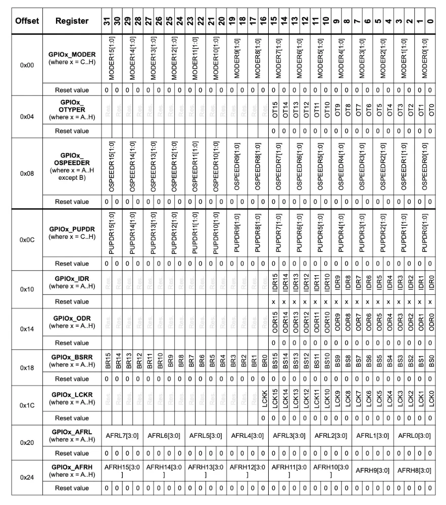
The registers fall into three groups. The first four registers configure the electrical behavior of each pin. IDR, ODR, and BSRR handle the data of the pin, and the two AFR registers select the alternate function. The LCKR register can freeze the configuration of a pin until the next reset. It is rarely used, so this article does not cover it. In CMSIS, the two alternate function registers form an array called AFR, where AFR[0] is AFRL and AFR[1] is AFRH.
Enabling the Port Clock
Before any of these registers can be used, the clock of the port must be enabled in the RCC peripheral. On the STM32F4 series, the GPIO ports are connected to the AHB1 bus, and the clock is enabled with the register RCC->AHB1ENR. A write to a GPIO register while the port clock is off has no effect.
|
1 |
RCC->AHB1ENR |= RCC_AHB1ENR_GPIOAEN; // Enable the clock of GPIOA |
The HAL macro __HAL_RCC_GPIOA_CLK_ENABLE() performs the same operation, and CubeMX places it in the generated GPIO initialization code.
STM32 GPIO Configuration Registers
These four registers configure how each pin behaves electrically, and the function HAL_GPIO_Init() writes all of them. The mode, speed, and pull registers use two bits per pin, while the output type register uses one bit per pin. The table below summarises the values of each field.
| Register | Bits per pin | Field values |
|---|---|---|
| MODER | 2 | 00 input 01 general purpose output 10 alternate function 11 analog |
| OTYPER | 1 | 0 push-pull 1 open-drain |
| OSPEEDR | 2 | 00 low 01 medium 10 fast 11 high |
| PUPDR | 2 | 00 no pull 01 pull-up 10 pull-down 11 reserved |
MODER
The mode register decides what the pin is used for. A pin in input mode reads the voltage that is present on it. A pin in output mode is driven by the output data register. A pin in alternate function mode is driven by a peripheral, and a pin in analog mode is disconnected from the digital circuits so that the ADC or DAC can use it. The field of pin n sits at the bits 2n+1 and 2n, which means that pin 5 uses the bits 11 and 10. The diagram below shows this layout.
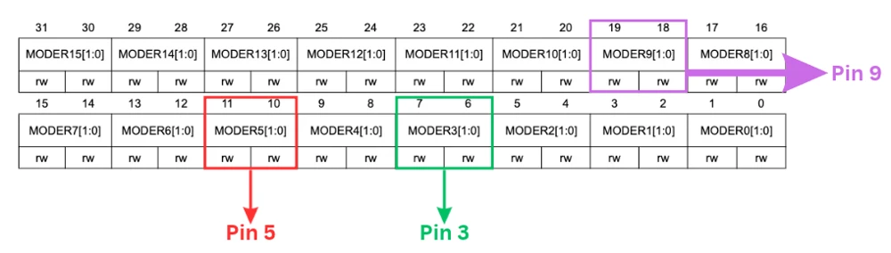
After a reset, most pins are in input mode with the value 00. The debug pins are an exception, because the pins used by the SWD interface start in alternate function mode. The register MODER of GPIOA therefore has the reset value 0xA8000000 and not zero.
OTYPER
The output type register selects between push-pull and open-drain for every pin that acts as an output. The value 0 selects push-pull, which can drive the pin both high and low. The value 1 selects open-drain, which can only pull the pin low and leaves the high level to an external or internal pull-up resistor. Only the lower 16 bits of this register are used, and the upper half is reserved. The reasons for choosing one type over the other are explained in the push-pull vs open-drain article.

OSPEEDR
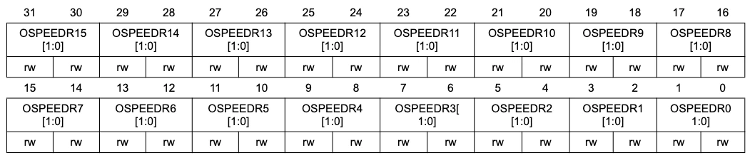
The output speed register controls how quickly the output driver changes the voltage of the pin. The four values we can choose from are low, medium, fast, and high. A higher setting gives steeper edges, which a fast signal such as an SPI clock needs. The actual frequency range of each setting depends on the supply voltage and the capacitive load, and the datasheet lists these values. Remeber that a higher setting also increases the noise and the power consumption, so the lowest setting that works is the best choice. The details are covered in the GPIO speed article.
PUPDR
The pull register connects an internal resistor to the pin. The value 01 enables the pull-up, the value 10 enables the pull-down, and the value 00 leaves the pin without a pull. These resistors are weak, with values in the range of tens of kilohm. They are mainly used to give a defined level to an input that would otherwise float and reading them would result in random values. The pull-up and pull-down article explains how to choose between them.

STM32 GPIO Data Registers (IDR and ODR)
The two data registers hold the logic levels of the pins. Only the lower 16 bits are used in both of them, and bit n belongs to pin n.
IDR
The input data register is read-only, and it shows the logic level that is present on each pin. The hardware samples the pins on every clock cycle of the AHB1 bus, so a read always returns the recent state. The register shows the real voltage on the pin, which makes it the correct source for reading a button or an open-drain bus. It also works when the pin is configured as an output.

The example below reads the user button B1 of the NUCLEO-F446RE board, which is connected to PC13 and gives a low level when it is pressed.
|
1 2 3 4 |
if ((GPIOC->IDR & GPIO_PIN_13) == 0U) { /* The button is pressed */ } |
ODR
The output data register is readable and writable, and it holds the value that the pin drives when it is configured as a general purpose output. When the pin is in input mode or in alternate function mode, the value in this register has no effect on the pin. A read of ODR returns the value that was written last. It does not return the voltage of the pin, which can differ, for example when an open-drain output is held low by another device on the bus.

The register can be written as a whole or bit by bit. A direct assignment such as GPIOA->ODR = 0x0020; changes all sixteen pins of the port at once, which is usually not the intention. The operators |=, &=, and ^= change single bits, but they are read-modify-write operations. The next section explains why this matters.
STM32 BSRR Register
The bit set and reset register is the preferred way to change the output of single pins. It is a 32-bit register that can only be written. The lower half contains the set bits BS0 to BS15, and the upper half contains the reset bits BR0 to BR15. A 1 in a set bit drives the corresponding pin high, and a 1 in a reset bit drives it low. A 0 in either half has no effect on the pin. If both bits of the same pin are written as 1 in one operation, the set bit wins. The diagram below shows the layout.
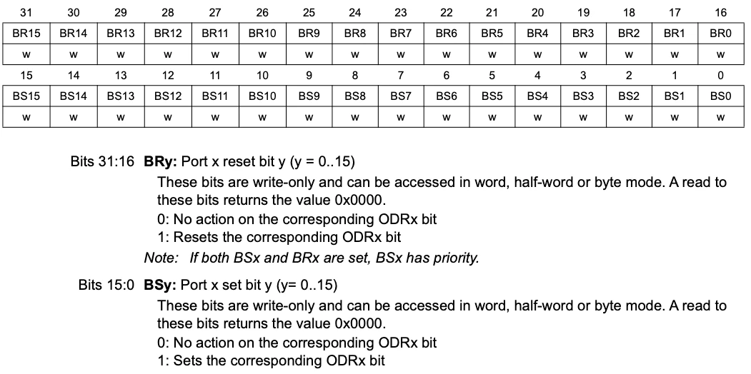
The following two lines set and reset the pin PA5. The cast to uint32_t before the shift keeps the operation safe for the pins with high numbers, such as GPIO_PIN_15, where the shifted value would not fit into a signed integer.
|
1 2 |
GPIOA->BSRR = GPIO_PIN_5; // Set PA5 GPIOA->BSRR = (uint32_t)GPIO_PIN_5 << 16U; // Reset PA5 |
Atomic Pin Control
The main advantage of BSRR is that a single write changes only the selected pins, and the CPU does not need to read the register first. An operation such as GPIOA->ODR |= GPIO_PIN_5; consists of three steps:
- Read ODR Register
- Change the value in a CPU register
- Write the updated data back
If an interrupt occurs between the read and the write, and the interrupt routine changes another pin of the same port, the main code writes back the old value and removes the change of the interrupt. This kind of error is rare and hard to reproduce, but it is possible in theory.
A write to BSRR consists of one step, so no interrupt can fall inside it, and the other pins of the port are never touched. This is why the HAL function HAL_GPIO_WritePin() is built on BSRR. A single write can also set some pins and reset others at the same moment, for example GPIOA->BSRR = GPIO_PIN_5 | ((uint32_t)GPIO_PIN_6 << 16U);, which sets PA5 and resets PA6 together.
STM32 AFR Alternate Function Registers
The alternate function registers select which peripheral signal is connected to a pin. Each pin has a four-bit field, which allows the values AF0 to AF15. The register AFRL holds the fields of the pins 0 to 7, and AFRH holds the fields of the pins 8 to 15. In CMSIS, these two registers are accessed as AFR[0] and AFR[1].
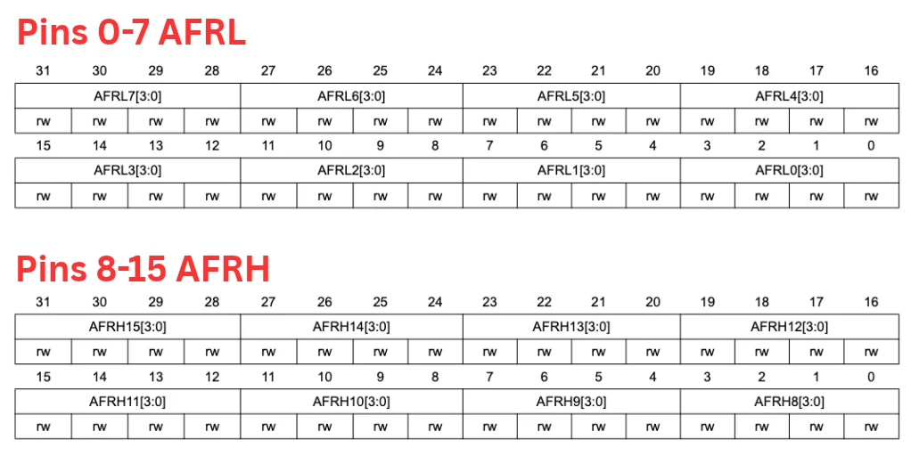
The AFR field works together with the mode field in MODER. The pin must be set to alternate function mode with the value 1 0 before the AFR value has any effect, and then the AFR value decides which peripheral signal reaches the pin through the multiplexer. The example below routes the signal USART1_TX to the pin PA9, which uses AF7 on the STM32F4 series. Pin 9 is the second field of AFRH, so the index of the field is 9 minus 8.
|
1 2 3 4 |
GPIOA->MODER &= ~(3U << (9U * 2U)); // Clear the 2-bit mode field of pin 9 (bits 19:18) GPIOA->MODER |= (2U << (9U * 2U)); // Set the field to 10 for alternate function mode GPIOA->AFR[1] &= ~(0xFU << ((9U - 8U) * 4U)); // Clear the 4-bit AF field of pin 9 in AFRH (bits 7:4) GPIOA->AFR[1] |= (7U << ((9U - 8U) * 4U)); // Set the field to 7, which selects AF7 = USART1_TX |
The AF numbers depend on the device, and they must be taken from the alternate function table of the datasheet. The alternate function pins article explains how to read this table and how CubeMX selects the numbers.
How Registers Work Together
A GPIO pin is controlled by all of the registers above at the same time, and each register affects a different part of the pin circuit. The diagram below shows a simplified view of one pin. The output path runs from the left to the pin, and the input path returns from the pin to the register IDR.
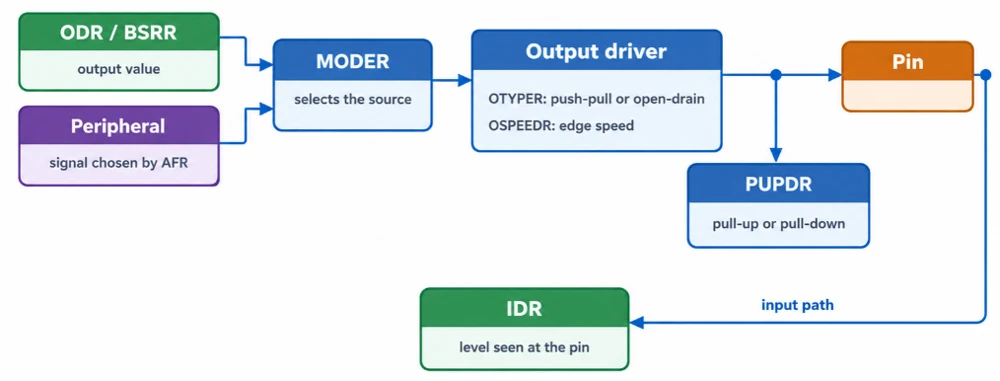
On the output path, ODR and BSRR provide the value, and the peripheral signal is the alternative source. The register MODER decides which of the two sources controls the driver, and the register AFR decides which peripheral signal is used when the alternate source is selected. The driver itself is configured by OTYPER, which sets the type of the output stage, and by OSPEEDR, which sets the steepness of the edges. The register PUPDR connects the pull resistor to the pin, and it acts on the pin independently of the driver. On the input path, the voltage of the pin is sampled and stored in IDR. The table below lists the question that each register answers.
| Register | Question it answers |
|---|---|
| MODER | What mode is the pin in? |
| OTYPER | What type of output stage does the pin use? |
| OSPEEDR | How fast are the edges of the output? |
| PUPDR | Which pull resistor is connected? |
| ODR and BSRR | What value does the output drive? |
| IDR | What value is present at the pin? |
| AFR | Which alternate function is connected? |
As an example, an LED output uses:
- MODER with the value 01
- OTYPER with 0 for push-pull
- the low speed setting
- no pull resistor
- BSRR for the output value.
Similarly, an I²C line uses:
- MODER with the value 10
- OTYPER with 1 for open-drain
- a pull-up
- the AF number of the I²C peripheral in AFR
HAL vs Register-Level GPIO
The HAL call and the register write below perform the same operation on the pin.
|
1 2 3 4 5 |
// HAL HAL_GPIO_WritePin(GPIOA, GPIO_PIN_5, GPIO_PIN_SET); // Registers GPIOA->BSRR = GPIO_PIN_5; |
The body of HAL_GPIO_WritePin() in the STM32F4 HAL checks its parameters when assertions are enabled, tests the requested state, and then writes either the pin mask or the pin mask shifted by 16 bits to BSRR. The register version removes the function call and the checks, and it leaves only the final write. This difference is small, but it can matter in code that toggles a pin at a high rate, or in a project that is very tight on code size.
The trade-off is portability and safety against speed and control. HAL code is readable and works on many STM32 families without changes, and it is tested by ST. It also keeps the application independent of the register names of one device. Register code is shorter and faster, and it gives direct control over each bit. However, it ties the code to one family and makes every bit position a responsibility of the programmer.
None of this means that you should avoid HAL. HAL is a good choice for most projects, and many professional products use it. The register level is best seen as a skill that supports HAL. It helps us to understand the driver, to debug it, and to step down to the registers in the few places where timing or code size requires it. The HAL vs LL article describes the LL library, which sits between the two approaches.
STM32 Register Bit Manipulation
Register programming relies on a small set of bit operations. Once these are clear, every register description in the reference manual becomes easier to use.
Masks and Shifts
A bit mask is a number that has a 1 in each bit position that should be changed. The shift operator creates a mask for a single bit, because 1U << 5U gives the value 0x20, which is the same as GPIO_PIN_5. The constant GPIO_PIN_5 is therefore a mask, and it is not the number 5. For the registers with a two-bit field, the mask 3U is shifted by the pin number multiplied by two, and for the registers with a four-bit field, the mask 0xFU is shifted by the pin number multiplied by four.
Read-Modify-Write
Most changes to a register follow the read-modify-write pattern. The code reads the current value, changes only the required bits, and writes the result back, so that the other bits keep their values. The table below shows the four basic operations with a register called REG.
| Operation | Code | Effect |
|---|---|---|
| Set bits | REG |= mask; | The bits in the mask become 1 |
| Clear bits | REG &= ~mask; | The bits in the mask become 0 |
| Toggle bits | REG ^= mask; | The bits in the mask are inverted |
| Test bits | REG & mask | Gives a non-zero value if any masked bit is 1 |
A field with several bits must be cleared before the new value is set. The reason is that the OR operation can only add ones. If a pin is in analog mode with the field value 11, and the code only sets the value 01 with an OR, the field stays at 11 and the pin stays in analog mode. The correct sequence clears the field with the mask first and then sets the new value, as in the MODER example in the working example below.
GPIO Register Example
This example controls the green LED LD2 of the NUCLEO-F446RE board with registers only. The LED is connected to the pin PA5. We will configure the pin as a push-pull output with low speed and no pull resistor, and then blink the LED once per second using BSRR.
Step 1: Create the Project
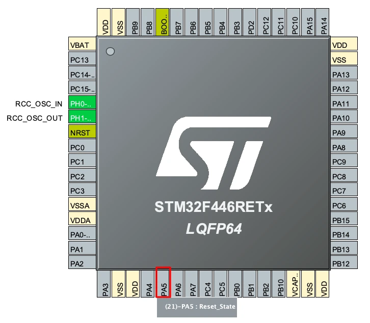
Create a new STM32CubeIDE project for the NUCLEO-F446RE board. Configure the clock as per your requirement, Read STM32 Clock System Explained if you are new to clock configuration. In the Pinout & Configuration tab, leave pin PA5 to Reset_State. This stops CubeMX from generating the HAL configuration of the pin, so the registers are the only code that configures it. Then generate the code.
Step 2: Enable the Port Clock
Open main.c and add the following lines between the USER CODE BEGIN 2 and USER CODE END 2 markers inside the main() function. The read of the same register after the write gives the clock a short time to become active before the first GPIO access.
|
1 2 3 |
/* USER CODE BEGIN 2 */ RCC->AHB1ENR |= RCC_AHB1ENR_GPIOAEN; // Enable the clock of GPIOA so its registers can be accessed (void)RCC->AHB1ENR; // Read the register back to give the clock a short time to start |
Step 3: Configure PA5
Add the configuration for the four registers directly below the clock enable. Every line clears the field of pin 5 first, and the second MODER line then sets the new value. The registers OTYPER, OSPEEDR, and PUPDR are cleared only, because the value 0 selects push-pull, low speed, and no pull.
|
1 2 3 4 5 6 |
GPIOA->MODER &= ~(3U << (5U * 2U)); // Clear the 2-bit mode field of pin 5 (bits 11:10) GPIOA->MODER |= (1U << (5U * 2U)); // Set the field to 01 for general purpose output mode GPIOA->OTYPER &= ~(1U << 5U); // Clear bit 5 to select push-pull output type GPIOA->OSPEEDR &= ~(3U << (5U * 2U)); // Clear the 2-bit speed field of pin 5 to select low speed GPIOA->PUPDR &= ~(3U << (5U * 2U)); // Clear the 2-bit pull field of pin 5 to select no pull resistor /* USER CODE END 2 */ |
Step 4: Control the LED
Inside the main while loop, set the pin with BSRR, wait for 1000 ms, reset the pin with the shifted value, and wait again. HAL_Delay() is still available, because HAL_Init() configures the SysTick timer before the user code runs.
|
1 2 3 4 5 6 7 8 9 10 |
while (1) { /* USER CODE END WHILE */ /* USER CODE BEGIN 3 */ GPIOA->BSRR = GPIO_PIN_5; // LED on HAL_Delay(1000); GPIOA->BSRR = (uint32_t)GPIO_PIN_5 << 16U; // LED off HAL_Delay(1000); } /* USER CODE END 3 */ |
Step 5: Result
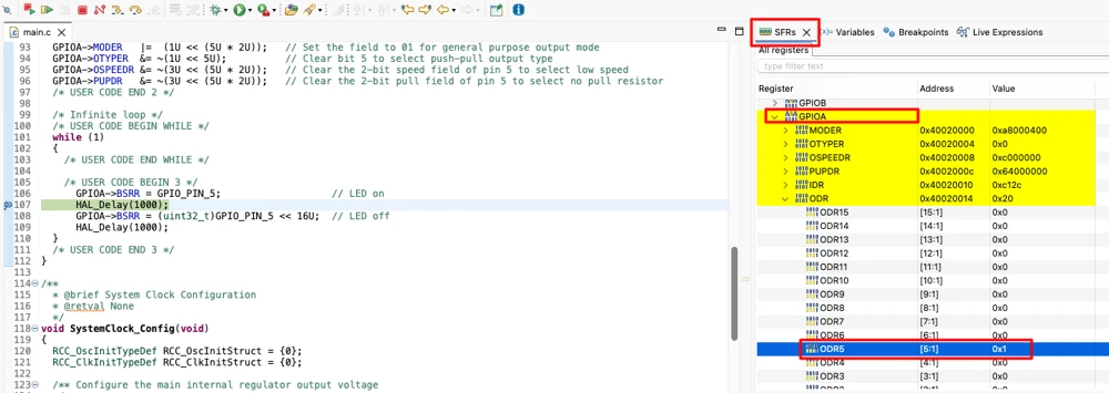
After the project is built and flashed, the LED LD2 blinks every 2 seconds.
To see the registers working, start a debug session, pause the program, and open the SFRs view of STM32CubeIDE. Under GPIOA, the field MODER5 shows the value 01, and the bit ODR5 changes between 0 and 1 as the program runs.
Conclusion
The GPIO registers are the layer where every HAL call ends. The registers MODER, OTYPER, OSPEEDR, and PUPDR configure the mode, the output type, the speed, and the pull resistor of each pin. The registers IDR and ODR hold the input and output values, BSRR changes single output bits in one atomic write, and the two AFR registers connect a pin to a peripheral signal. Together they control the complete circuit of a pin, from the output value to the driver and from the pin back to the input register.
Working at this level depends on careful bit manipulation. The pin number has to be turned into the correct shift for each register, multi-bit fields have to be cleared before they are set, and BSRR should be used for single pin changes. The registers also differ between STM32 families, so the reference manual of the exact device is the final source of every address, field, and clock enable bit. HAL remains a good choice for most work, and the knowledge of the registers makes it easier to use, to debug, and to extend.
Download the Project Here
Download the CubeMX project files and HAL source code — all tested on real hardware.
If you find this useful, you can support us with a Donation as well.